
Datasheet


DS12885/DS12887/DS12887A/DS12C887/DS12C887A
Real-Time Clocks
6 _____________________________________________________________________
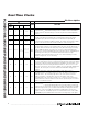
POWER-UP/POWER-DOWN CHARACTERISTICS
(T
A
= -40°C to +85°C) (Note 2)
PARAMETER SYMBOL CONDITIONS MIN TYP MAX UNITS
Recovery at Power-Up t
RPU
20 200 ms
V
CC
Fall Time; V
PF(MAX)
to
V
PF(MIN)
t
F
300 µs
V
CC
Rise Time; V
PF(MIN)
to
V
PF(MAX)
t
R
0µs
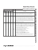
CAPACITANCE
(T
A
= +25°C) (Note 9)
PARAMETER SYMBOL CONDITIONS MIN TYP MAX UNITS
Capacitance on All Input Pins
Except X1 and X2
C
IN
5pF
Capacitance on IRQ, SQW, and
DQ Pins
C
IO
7pF
DATA RETENTION
(T
A
= +25°C)
PARAMETER SYMBOL CONDITIONS MIN TYP MAX UNITS
Expected Data Retention t
DR
10 years
AC TEST CONDITIONS
PARAMETER TEST CONDITIONS
Input Pulse Levels 0 to 3.0V
Output Load Including Scope and Jig 50pF + 1TTL Gate
Input and Output Timing Measurement Reference Levels Input/Output: V
IL
maximum and V
IH
minimum
Input-Pulse Rise and Fall Times 5ns
WARNING: Negative undershoots below -0.3V while the part is in battery-backed mode may cause loss of data.
Note 1: RTC modules can be successfully processed through conventional wave-soldering techniques as long as temperature
exposure to the lithium energy source contained within does not exceed +85°C. However, post-solder cleaning with water-
washing techniques is acceptable, provided that ultrasonic vibrations are not used to prevent crystal damage.
Note 2: Limits at -40°C are guaranteed by design and not production tested.
Note 3: All voltages are referenced to ground.
Note 4: All outputs are open.
Note 5: Specified with CS = DS = R/W = RESET = V
CC
; MOT, AS, AD0–AD7 = 0; V
BACKUP
open.
Note 6: Applies to the AD0 to AD7 pins, the IRQ pin, and the SQW pin when each is in a high-impedance state.
Note 7: The MOT pin has an internal 20kΩ pulldown.
Note 8: Measured with a 32.768kHz crystal attached to X1 and X2.
Note 9: Guaranteed by design. Not production tested.
Note 10: Measured with a 50pF capacitance load.