
Datasheet
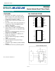

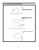

DS1306
2 of 22
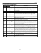
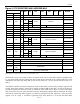
ORDERING INFORMATION
PART TEMP RANGE PIN-PACKAGE TOP MARK*
DS1306 0°C to +70°C 16 DIP (300 mils) DS1306
DS1306+ 0°C to +70°C 16 DIP (300 mils) DS1306 +
DS1306N -40°C to +85°C 16 DIP (300 mils) DS1306N
DS1306N+ 0°C to +70°C 16 DIP (300 mils) DS1306N +
DS1306E 0°C to +70°C 20 TSSOP (173 mils) DS1306
DS1306E+ 0°C to +70°C 20 TSSOP (173 mils) DS1306 +
DS1306EN -40°C to +85°C 20 TSSOP (173 mils) DS1306N
DS1306EN+ -40°C to +85°C 20 TSSOP (173 mils) DS1306N +
DS1306EN/T&R -40°C to +85°C 20 TSSOP (173 mils) DS1306N
DS1306EN+T&R -40°C to +85°C 20 TSSOP (173 mils) DS1306N +
DS1306E/T&R 0°C to +70°C 20 TSSOP (173 mils) DS1306
DS1306E+T&R 0°C to +70°C 20 TSSOP (173 mils) DS1306 +
+Denotes a lead(Pb)-free/RoHS-compliant package
T&R = Tape and reel.
*An “N” on the top mark indicates an industrial device.
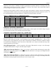
PIN DESCRIPTION
PIN
TSSOP DIP
NAME FUNCTION
1 1 V
CC2
Backup Power Supply. This is the secondary power supply pin. In systems
using the trickle charger, the rechargeable energy source is connected to this
pin.
2 2 V
BAT
Battery Input for Any Standard +3V Lithium Cell or Other Energy
Source. If not used, V
BAT
must be connected to ground. Diodes must not be
placed in series between V
BAT
and the battery, or improper operation will
result. UL recognized to ensure against reverse charging current when used
in conjunction with a lithium battery. See “Conditions of Acceptability” at
www.maxim-ic.com/TechSupport/QA/ntrl.htm
.
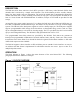
3 3 X1
5 4 X2
Connections for Standard 32.768kHz Quartz Crystal. The internal
oscillator is designed for operation with a crystal having a specified load
capacitance of 6pF. For more information on crystal selection and crystal
layout considerations, refer to Application Note 58, “Crystal Considerations
with Dallas Real-Time Clocks.” The DS1306 can also be driven by an
external 32.768kHz oscillator. In this configuration, the X1 pin is connected
to the external oscillator signal and the X2 pin is floated.
7 5
INT0
Active-Low Interrupt 0 Output. The INT0 pin is an active-low output of
the DS1306 that can be used as an interrupt input to a processor. The INT0
pin can be programmed to be asserted by Alarm 0. The INT0 pin remains
low as long as the status bit causing the interrupt is present and the
corresponding interrupt enable bit is set. The INT0 pin operates when the
DS1306 is powered by V
CC1
, V
CC2
, or V
BAT
. The INT0 pin is an open-drain
output and requires an external pullup resistor.
8 6 INT1
Interrupt 1 Output. The INT1 pin is an active-high output of the DS1306
that can be used as an interrupt input to a processor. The INT1 pin can be
programmed to be asserted by Alarm 1. When an alarm condition is present,
the INT1 pin generates a 62.5ms active-high pulse. The INT1 pin operates
only when the DS1306 is powered by V
CC2
or V
BAT
. When active, the INT1
pin is internally pulled up to V
CC2
or V
BAT
. When inactive, the INT1 pin is
internally pulled low.