
Datasheet
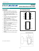


DS1306
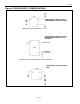
8 of 22
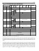
STATUS REGISTER (READ 10H)
BIT7 BIT6 BIT5 BIT4 BIT3 BIT2 BIT1 BIT0
0 0 0 0 0 0 IRQF1 IRQF0
IRQF0 (Interrupt 0 Request Flag) – A logic 1 in the interrupt request flag bit indicates that the current
time has matched the Alarm 0 registers. If the AIE0 bit is also a logic 1, the
INT0 pin goes low. IRQF0 is
cleared when the address pointer goes to any of the Alarm 0 registers during a read or write. IRQF0 is
activated when the device is powered by V
CC1
, V
CC2
, or V
BAT
.
IRQF1 (Interrupt 1 Request Flag) – A logic 1 in the interrupt request flag bit indicates that the current
time has matched the Alarm 1 registers. If the AIE1 bit is also a logic 1, the INT1 pin generates a 62.5ms
active-high pulse. IRQF1 is cleared when the address pointer goes to any of the alarm 1 registers during a
read or write. IRQF1 is activated only when the device is powered by V
CC2
or V
BAT
.
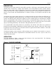
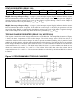
TRICKLE CHARGE REGISTER (READ 11H, WRITE 91H)
This register controls the trickle charge characteristics of the DS1306. The simplified schematic of Figure
3 shows the basic components of the trickle charger. The trickle charge select (TCS) bits (bits 4–7)
control the selection of the trickle charger. In order to prevent accidental enabling, only a pattern of 1010
enables the trickle charger. All other patterns disable the trickle charger. The DS1306 powers up with the
trickle charger disabled. The diode select (DS) bits (bits 2–3) select whether one diode or two diodes are
connected between V
CC1
and V
CC2
. The diode select (DS) bits (bits 2–3) select whether one diode or two
diodes are connected between V
CC1
and V
CC2
. The resistor select (RS) bits select the resistor that is
connected between V
CC1
and V
CC2
. The resistor and diodes are selected by the RS and DS bits as shown
in Table 3.
Figure 3. PROGRAMMABLE TRICKLE CHARGER