
Datasheet

DS1307 64 x 8, Serial, I
2
C Real-Time Clock
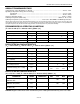
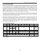
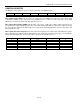
AC ELECTRICAL CHARACTERISTICS
(V
CC
= 4.5V to 5.5V; T
A
= 0°C to +70°C, T
A
= -40°C to +85°C.)
PARAMETER SYMBOL CONDITIONS MIN TYP MAX UNITS
SCL Clock Frequency f
SCL
0 100 kHz
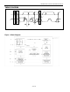
Bus Free Time Between a STOP and
START Condition
t
BUF
4.7
µs
Hold Time (Repeated) START
Condition
t
HD:STA
(Note 4) 4.0
µs
LOW Period of SCL Clock t
LOW
4.7
µs
HIGH Period of SCL Clock t
HIGH
4.0
µs
Setup Time for a Repeated START
Condition
t
SU:STA
4.7
µs
Data Hold Time t
HD:DAT
0
µs
Data Setup Time t
SU:DAT
(Notes 5, 6) 250 ns
Rise Time of Both SDA and SCL
Signals
t
R
1000 ns
Fall Time of Both SDA and SCL
Signals
t
F
300 ns
Setup Time for STOP Condition t
SU:STO
4.7
µs
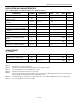
CAPACITANCE
(T
A
= +25°C)
PARAMETER SYMBOL CONDITIONS MIN TYP MAX UNITS
Pin Capacitance (SDA, SCL) C
I/O
10 pF
Capacitance Load for Each Bus
Line
C
B
(Note 7) 400 pF
Note 1:
All voltages are referenced to ground.
Note 2:
Limits at -40°C are guaranteed by design and are not production tested.
Note 3:
I
CCS
specified with V
CC
= 5.0V and SDA, SCL = 5.0V.
Note 4:
After this period, the first clock pulse is generated.
Note 5:
A device must internally provide a hold time of at least 300ns for the SDA signal (referred to the V
IH(MIN)
of the SCL
signal) to bridge the undefined region of the falling edge of SCL.
Note 6:
The maximum t
HD:DAT
only has to be met if the device does not stretch the LOW period (t
LOW
) of the SCL signal.
Note 7:
C
B
—total capacitance of one bus line in pF.
3 of 14