
Datasheet


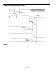

DS1314
10 of 12
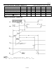
NOTES:
2. All voltages referenced to ground.
3. Measured with outputs open circuited.
4. I
CCO1
is the maximum average load which the DS1314 can supply to attached memories at V
CCO
≥
V
CCI
-0.2V.
5. I
CCO1
is the maximum average load which the DS1314 can supply to attached memories at V
CCO
≥
V
CCI
-0.3V.
6. All inputs within 0.3V of ground or V
CCI
.
7. I
CCO2
is the maximum average load current which the DS1314 can supply to the memories in the
battery-backup mode.
8. Measured with a load as shown in Figure 2.
9. Chip Enable Output (
CEO
) can only sustain leakage current in the battery-backup mode.
10.
CEO
will be held high for a time equal to t
REC
after V
CCI
crosses V
CCTP
on power-up.
11.
BW
and
RST
are open drain outputs and as such cannot source current. External pull-up resistors
should be connected to these pins for proper operation. Both
BW
and
RST
can sink 10 mA.
12. t
CE
maximum must be met to ensure data integrity on power-down.
13. In battery-backup mode, inputs must never be below ground or above V
CCO
.
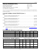
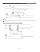
DC TEST CONDITIONS
Outputs Open
All voltages are referenced to ground
AC TEST CONDITIONS
Output Load: See below
Input Pulse Levels: 0 - 3.0V
Timing Measurement Reference Levels
Input: 1.5V
Output: 1.5V
Input pulse Rise and Fall Times: 5 ns
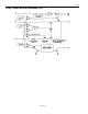
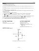
OUTPUT LOAD Figure 2
* INCLUDING SCOPE AND JIG CAPACITANCE