
Datasheet


DS1314
12 of 12
Maxim cannot assume responsibility for use of any circuitry other than circuitry entirely embodied in a Maxim product. No circuit patent licenses are implied. Maxim
reserves the right to change the circuitry and specifications without notice at any time.
Maxim Integrated Products, Inc. 160 Rio Robles, San Jose, CA 95134 USA 1-408-601- 1000
© 2012 Maxim Integrated Products Maxim is a registered trademark of Maxim Integrated Products, Inc.
DATA SHEET REVISION SUMMARY
The following represent the key differences between 12/16/96 and 06/12/97 version of the DS1314 data
sheet. Please review this summary carefully.
1. Changed V
BAT
max to 6V.
2. Changed V
CCTP
values to 2.8 - 3.0V (TOL = GND) and 2.5 - 2.7V (TOL = V
CC
).
3. Changed t
BABW
from 7s to 1s max.
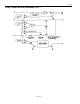
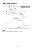
4. Changed block diagram to show U L compliance.
The following represent the key differences between 06/12/97 and 08/29/97 version of the DS1314 data
sheet. Please review this summary carefully.
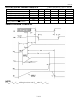
1. Changed AC test conditions.
2. Changed t
PD
to 20 max & 12 typ.
The following represent the key differences between 08/29/97 and 12/16/97 version of the DS1314 data
sheet. Please review this summary carefully.
1. Changed V
CCI
mins from 3.05V to 3.0V (TOL=GND) and from 275V to 2.7V (TOL=V
CCD
) (this
should have been done on 06/12/97 revision but was overlooked).
2. Specified Input Capacitance as being only for
CEI
, TOL and Output Capacitance as being only for
CEO
,
BW
and
RST
. This is not a change but rather clarification.
3. Removed “preliminary” from title bar.
The following represent the key differences between 12/16/97 and 6/12 version of the DS1314 data sheet.
Please review this summary carefully.
1. Update soldering, ordering, package information, and notes.