
Datasheet


DS1803
8 of 11
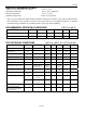
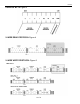
5. After this period, the first clock pulse is generated.
6. A device must internally provide a hold time of at least 300 ns for the SDA signal (referred to the
V
IHMIN
of the SCL signal) in order to bridge the undefined region of the falling edge of SCL.
7. The maximum t
HD:DAT
has only to be met if the device does not stretch the LOW period (t
LOW
) of the
SCL signal.
8. A fast mode device can be used in a standard mode system, but the requirement t
SU:DAT
> 250 ns must
then be met. This will automatically be the case if the device does not stretch the LOW period of the
SCL signal. If such a device does stretch the LOW period of the SCL signal, it must output the next
data bit to the SDA line t
RMAX
+ t
SU:DAT
= 1000 + 250=1250 ns before the SCL line is released.
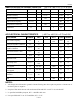
9. C
B
- total capacitance of one bus line in picofarads, timing referenced to (0.9)(V
CC
) and (0.1)(V
CC
).
10. Typical values are for t
A
= 25°C and nominal supply voltage.
11. -3 dB cutoff frequency characteristics for the DS1803 depend on potentiometer total resistance:
DS1803-010; 1 MHz, DS1803-50; 200 kHz, DS1803-100; 100 kHz.
12. Address Inputs, A0, A1, and A2, should be tied to either V
CC
or GND depending on the desired
address selections.
13. Absolute linearity is used to determine wiper voltage versus expected voltage as determined by wiper
position. Device test limits are ±1.6 LSB.
14. Relative linearity is used to determine the change in voltage between successive tap positions. Device
test limits ±0.5 LSB.
15. Fast mode.
16. Standard mode.
17. Valid at 25°C only.