
Datasheet


35Maxim Integrated
SFP Controller for Dual Rx Interface
DS1877
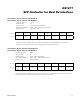
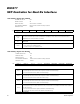
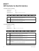
Lower Memory, Register 6Eh: STATUS
POWER-ON VALUE X0XX 0XXXb
READ ACCESS All
WRITE ACCESS See below
A2h AND B2h MEMORY Mixture of common memory locations and different memory locations (see below)
MEMORY TYPE Volatile
Write
Access
N/A All N/A All All N/A N/A N/A
6Eh RESERVED
<5/D>
TXDC
<2/C>
INXS
<2/C>
RSELS
<5/C>
RSELC
<2/C>
FLTS
<2/D>
RXL
<2/C>
RDYB
BIT 7 BIT 0
BIT 7 RESERVED
BIT 6
TXDC1 [A2h]: TXD1 software control bit (writable by all users).
0 = (default) This bit has no effect on alarms and warnings.
1 = Setting TXDC1 inhibits the latching of low alarms and warnings LOS1 LO, LOS2 LO, RSSI1
LO, and RSSI2 LO after the condition is cleared. Once TXDC1 is set, it is internally extended by
time t
INITR
to allow for settings to stabilize. Clearing TXDC1 before t
INITR
has no impact on the
latching of these alarms and warnings.
TXDC2 [B2h]: TXD2 software control bit (writable by all users).
0 = (default) This bit has no effect on alarms and warnings.
1 = Setting TXDC2 inhibits the latching of low alarms and warnings LOS1 LO, LOS2 LO, RSSI1
LO, and RSSI2 LO after the condition is cleared. Once TXDC2 is set, it is internally extended by
time t
INITR
to allow for settings to stabilize. Clearing TXDC2 before t
INITR
has no impact on the
latching of these alarms and warnings.
BIT 5
INXS [A2h or B2h]: INX status bit. Reflects the logic state of the INX pin (read-only).
0 = INX pin is logic-low.
1 = INX pin is logic-high.
BIT 4
RSELS [A2h or B2h]: RSEL status bit. Reflects the logic state of the RSEL pin (read-only).
0 = RSEL pin is logic-low.
1 = RSEL pin is logic-high.
BIT 3
RSELC [A2h or B2h]: RSEL software control bit. This bit allows for software control that is iden-
tical to the RSEL pin. Its value is wire-ORed with the logic value of the RSEL pin to create the
RSELOUT pin’s logic value (writable by all users).
0 = (default)
1 = Forces the device into a RSEL state regardless of the value of the RSEL pin.
BIT 2
FLTS: Reflects the driven state of the FAULT pin (read-only).
0 = FAULT pin is low.
1 = FAULT pin is high.
BIT 1
RXL1 [A2h]: Status of LOS1 pin or LOS1 LO as determined by the LOSC control bit.
RXL2 [B2h]: Status of LOS2 pin or LOS2 LO as determined by the LOSC control bit.
BIT 0
RDYB [A2h or B2h]: Ready bar.
0 = V
CC
is above POA.
1 = V
CC
is below POA and/or too low to communicate over the I
2
C bus.