
Datasheet


40 Maxim Integrated
SFP Controller for Dual Rx Interface
DS1877
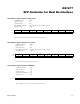
Table 01h Register Descriptions
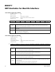
Table 01h, Register 80h–F7h: EEPROM
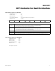
Table 01h, Register F8h: ALARM EN
3
POWER-ON VALUE 00h
READ ACCESS PW2 or (PW1 and RWTBL1A) or (PW1 and RTBL1A)
WRITE ACCESS PW2 or (PW1 and RWTBL1A)
A2h AND B2h MEMORY Common A2h and B2h memory locations
MEMORY TYPE Nonvolatile (EE)
80h–F7h EE EE EE EE EE EE EE EE
BIT 7 BIT 0
EEPROM for PW1 and/or PW2 level access.
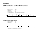
POWER-ON VALUE 00h
READ ACCESS PW2 or (PW1 and RWTBL1C) or (PW1 and RTBL1C)
WRITE ACCESS PW2 or (PW1 and RWTBL1C)
A2h AND B2h MEMORY Common A2h and B2h memory locations
MEMORY TYPE Nonvolatile (SEE)
F8h TEMP HI TEMP LO VCC HI VCC LO RESERVED RESERVED RESERVED RESERVED
BIT 7 BIT 0
Layout is identical to ALARM
3
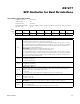
in Lower Memory, Register 70h. Enables alarms to create FLTINT (Lower Memory,
Register 71h) logic. The MASK bit (Table 02h, Register 88h) determines whether this memory exists in Table 01h or 05h.
BIT 7
TEMP HI [A2h or B2h]:
0 = Disables interrupt from TEMP HI alarm.
1 = Enables interrupt from TEMP HI alarm.
BIT 6
TEMP LO [A2h or B2h]:
0 = Disables interrupt from TEMP LO alarm.
1 = Enables interrupt from TEMP LO alarm.
BIT 5
VCC HI [A2h or B2h]:
0 = Disables interrupt from VCC HI alarm.
1 = Enables interrupt from VCC HI alarm.
BIT 4
VCC LO [A2h or B2h]:
0 = Disables interrupt from VCC LO alarm.
1 = Enables interrupt from VCC LO alarm.
BITS 3:0 RESERVED