
Datasheet


DS1878
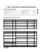
Stresses beyond those listed under “Absolute Maximum Ratings” may cause permanent damage to the device. These are stress ratings only, and functional
operation of the device at these or any other conditions beyond those indicated in the operational sections of the specifications is not implied. Exposure to
absolute maximum rating conditions for extended periods may affect device reliability.
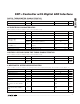
Voltage Range on MON1–MON4, RSEL, CSEL1OUT,
CSEL2OUT, SCLOUT, SDAOUT, TXDOUT, IN1,
LOS, TXF, TXFOUT, and TXD Pins
Relative to Ground .................................-0.5V to (V
CC
+ 0.5V)*
Voltage Range on V
CC
, SDA, SCL, RSELOUT,
and LOSOUT Pins Relative to Ground ..................-0.5V to +6V
Continuous Power Dissipation (T
A
= +70°C)
28 Pin TQFN (derate 34.5mW/°C above +70°C) .....2758.6mW
Operating Temperature Range ...........................-40°C to +95°C
Programming Temperature Range .........................0°C to +95°C
Storage Temperature Range .............................-55°C to +125°C
Lead Temperature (soldering, 10s) .................................+300°C
Soldering Temperature (reflow) .......................................+260°C
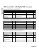
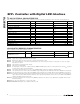
PARAMETER SYMBOL CONDITIONS MIN TYP MAX UNITS
Main Supply Voltage V
CC
(Note 1) 2.85 5.5 V
High-Level Input Voltage
(SDA, SCL, SDAOUT)
V
IH:1
0.7 x
V
CC
V
CC
+
0.3
V
Low-Level Input Voltage
(SDA, SCL, SDAOUT)
V
IL:1
-0.3
0.3 x
V
CC
V
High-Level Input Voltage
(TXD, TXF, RSEL, IN1, LOS)
V
IH:2
2.0
V
CC
+
0.3
V
Low-Level Input Voltage
(TXD, TXF, RSEL, IN1, LOS)
V
IL:2
-0.3 +0.8 V
DC ELECTRICAL CHARACTERISTICS
(V
CC
= +2.85V to +5.5V, T
A
= -40°C to +95°C, unless otherwise noted.)
*
Subject to not exceeding +6V.
RECOMMENDED OPERATING CONDITIONS
(T
A
= -40°C to +95°C, unless otherwise noted.)
ABSOLUTE MAXIMUM RATINGS
SFP+ Controller with Digital LDD Interface
_______________________________________________________________________________________ 5
PARAMETER SYMBOL CONDITIONS MIN TYP MAX UNITS
Supply Current I
CC
(Notes 1, 2) 2.5 4 mA
Output Leakage
(SDA, SDAOUT, RSELOUT,
LOSOUT, TXFOUT)
I
LO
1 μA
I
OL
= 4mA 0.4
Low-Level Output Voltage (SDA,
SDAOUT, SCLOUT, CSEL1OUT,
CSEL2OUT, RSELOUT, LOSOUT,
TXDOUT, DAC1, DAC2, TXFOUT)
V
OL
I
OL
= 6mA 0.6
V
High-Level Output Voltage
(DAC1, DAC2, SCLOUT,
SDAOUT, CSEL1OUT,
CSEL2OUT, TXDOUT)
V
OH
I
OH
= 4mA
V
CC
-
0.4
V
TXDOUT Before EEPROM Recall
DAC1 and DAC2 Before Recall
High impedance before recall 55 550 100 M
Input Leakage Current
(IN1, LOS, RSEL, SCL, TXD, TXF)
I
LI
1 μA
Digital Power-On Reset POD 1.0 2.2 V
Analog Power-On Reset POA 2.0 2.75 V