
Datasheet


DS1904
9 of 13
Skip ROM [CCh]
This command can save time in a single drop bus system by allowing the bus master to access the clock
f
unctions without providing the 64-bit ROM code. If more than one slave is present on the bus and, for
example, a read command is issued following the Skip ROM command, data collision will occur on the
bus as multiple slaves transmit simultaneously (open drain pull-downs will produce a wired-AND result).
1–WIRE SIGNALING
The DS1904 requires strict protocols to ensure data integrity. The protocol consists of four types of sig-
naling on one line: Reset Sequence with Reset Pulse and Presence Pulse, Write 0, Write 1 and Read Data.
Except for the presence pulse the bus master initiates all these signals.
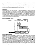
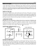
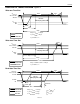
The initialization sequence required to begin any communication with the DS1904 is shown in Figure 8.
A reset pulse followed by a presence pulse indicates the DS1904 is ready to send or receive data. The bus
master transmits (TX) a reset pulse (t
RSTL
, minimum 480 µs
). The bus master then releases the line and
goes into receive mode (RX). The 1-Wire bus is pulled to a high state via the pull-up resistor. After
detecting the rising edge on the data line, the DS1904 waits (t
PDH
, 15-60 µs) and then transmits the
presence pulse (t
PDL
, 60-240 µs).
INITIALIZATION PROCEDURE “RESET AND PRESENCE PULSES” Figure 8
RESISTOR
MASTER
DS1904
MASTER RX "PRESENCE PULSE"
480 µs
≤
t
RSTL
<
∞
*
480 µs
≤
t
RSTH
<
∞
**
15 µs
≤
t
PDH
< 60 µs
60
≤
t
PDL
< 240 µs
MASTER TX
"RESET PULSE"
V
PULLUP
V
PULLUP MIN
V
IH MIN
V
IL MAX
0V
t
RSTH
t
RSTL
t
PDH
t
PDL
t
R
* In order not to mask interrupt signaling by other devices on the 1-Wire bus t
RSTL
+ t
R
should al-
ways be less than 960 µs.
** Includes recovery time
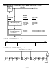
READ/WRITE TIME SLOTS
The definitions of write and read time slots are illustrated in Figure 9. The master initiates all time slots
by driving the data line low. The falling edge of the data line synchronizes the DS1904 to the master by
triggering an internal delay circuit. During write time slots, the delay circuit determines when the DS1904
will sample the data line. For a read data time slot, if a “0” is to be transmitted, the delay circuit deter-
mines how long the DS1904 will hold the data line low. If the data bit is a “1”, the DS1904 will not hold
the data line low at all.