
Datasheet


1. PIN DESCRIPTION
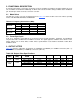
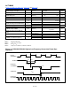
Table 1-A. Pin Description
PIN
DIP SO
NAME TYPE FUNCTION
—
1, 3, 6, 8, 10,
11, 13, 15
N.C. — No Connect
1 2 SYNCOUT Output
Synchronization Output. An 8kHz output that can be
synchronized to the clock outputs.
2 4 CLKOUT2 Output
Clock Output 2. T1 or E1 carrier clock output referenced to
CLKIN.
3 5 CLKIN Input
Clock Input. Reference Clock Input. CLKOUT1 and CLKOUT2
will be referenced to this clock.
4 7 CLKOUT1 Output
Clock Output 1. T1 or E1 carrier clock output referenced to
CLKIN.
5 9 Vss Supply Ground
6 12 SEL Input Clock Mode Select. Conversion mode select.
7 14 SYNCIN Input
Synchronization Input. Used to synchronize the clock outputs
and SYNCOUT to CLKIN and SYNCIN. SYNCIN should be tied
high or low when not in use.
8 16 V
DD
Supply Positive Supply, 3.3V or 5V ±5%
1.1 Pin Name Cross-Reference to LXP60X
Table 1-B. Pin Name Cross-Reference to LXP60x
DS21600/DS21602
/DS21604
LXP600ALXP602/L
XP604
FUNCTION
SYNCOUT FSO Synchronization Pulse Output
CLKOUT2 HFO Clock 2 Output
CLKIN CLKI Clock Input
CLKOUT1 CLKO Clock 1 Output
V
SS
GND Ground
SEL SEL Clock Mode Select
SYNCIN FSI Synchronization Pulse Input
N.C. N.C. No Connect
V
DD
V
CC
Positive Supply
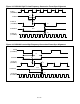
Figure 1-1. Block Diagram
ANALOG
PLL
OUTPUT
DIVIDER
FRAME SYNC
GENERATOR
CLKIN
SEL
SYNCIN
CLKOUT2
CLKOUT1
SYNCOUT
FEEDBACK
CIRCUIT
Dallas Semiconductor
DS21600/DS21602/DS21604
3 of 12