
Datasheet


DS2762 High-Precision Li+ Battery Monitor With Alerts
10 of 25
register, and enters sleep mode. The DS2762 provides a current-limited (I
RC
) recovery charge path from PLS to
V
DD
to gently charge severely depleted cells. The recovery path is enabled when 0 £ V
DD
< 3V (typ). Once V
DD
reaches 3V (typ), the DS2762 returns to normal operation, awaiting connection of a charger to turn on the charge
FET and pull out of sleep mode.
Overcurrent, Charge Direction. The voltage difference between the IS1 pin and the IS2 pin (V
IS
= V
IS1
-
V
IS2
) is the
filtered voltage drop across the current-sense resistor. If V
IS
exceeds overcurrent threshold V
OC
for a period longer
than overcurrent delay t
OCD
, the DS2762 shuts off both external FETs and sets the COC flag in the protection
register. The charge current path is not re-established until the voltage on the PLS pin drops below V
DD
- V
TP
. The
DS2762 provides a test current of value I
TST
from PLS to V
SS
to pull PLS down to detect the removal of the
offending charge current source.
Overcurrent, Discharge Direction. If V
IS
is less than -V
OC
for a period longer than t
OCD
, the DS2762 shuts off the
external discharge FET and sets the DOC flag in the protection register. The discharge current path is not re-
established until the voltage on PLS rises above V
DD
- V
TP
. The DS2762 provides a test current of value I
TST
from
V
DD
to PLS to pull PLS up to detect the removal of the offending low-impedance load.
Short Circuit. If the voltage on the SNS pin with respect to V
SS
exceeds short-circuit threshold V
SC
for a period
longer than short-circuit delay t
SCD
, the DS2762 shuts off the external discharge FET and sets the DOC flag in the
protection register. The discharge current path is not re-established until the voltage on PLS rises above V
DD
- V
TP
.
The DS2762 provides a test current of value I
TST
from V
DD
to PLS to pull PLS up to detect the removal of the short
circuit.
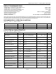
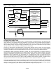
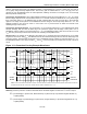
Figure 3. Li+ Protection Circuitry Example Waveforms
Summary. All of the protection conditions described above are ORed together to affect the
CC and DC outputs.
DC = (Undervoltage) or (Overcurrent, Either Direction) or (Short Circuit) or (Protection Register Bit DE = 0)
or (Sleep Mode)
CC = (Overvoltage) or (Undervoltage) or (Overcurrent, Charge Direction) or (Protection Register bit CE = 0)
or (Sleep Mode)
SLEEP
MODE
V
OV
V
CE
V
UV
V
CELL
V
IS
CHARGE
DISCHARGE
CC
DC
-V
SC
V
OC
-V
OC
0
t
SCD
t
OCD
t
OCD
t
UVD
t
OVD
V
PLS
V
DD
ACTIVE
V
SS
V
SS
INACTIVE
t
OVD
(NOTE 1)
NOTE 1: TO ALLOW THE DEVICE TO REACT QUICKLY TO SHORT CIRCUITS, DETECTION OCCURS ON THE SNS PIN RATHER THAN ON THE
FILTERED I
S
1 AND I
S
2 PIN
S
. THE A
C
T
U
AL
S
H
O
RT-
C
IR
CU
IT DETE
C
T
CO
NDITI
O
N I
S
V
SNS
> V
SC
.