
Datasheet


DS2762 High-Precision Li+ Battery Monitor With Alerts
2 of 25
ABSOLUTE MAXIMUM RATINGS
Voltage Range on PLS and CC Pin, Relative to V
SS
-0.3V to +18V
Voltage Range on PIO Pin, Relative to V
SS
-0.3V to +12V
Voltage Range on Any Other Pin, Relative to V
SS
-0.3V to +6V
Continuous Internal Sense Resistor Current
±2.5A
Pulsed Internal Sense Resistor Current
±50A for <100µs/s, <1000 pulses
Operating Temperature Range -40°C to +85°C
Storage Temperature Range -55°C to +125°C
Soldering Temperature See IPC/JEDEC J-STD-020A Specification
Stresses beyond those listed under “Absolute Maximum Ratings” may cause permanent damage to the device. These are stress ratings only,
and functional operation of the device at these or any other conditions beyond those indicated in the operational sections of the specifications is
not implied. Exposure to the absolute maximum rating conditions for extended periods may affect device.
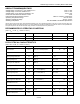
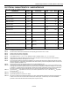
RECOMMENDED DC OPERATING CONDITIONS
(2.5V £ V
DD
£ 5.5V, T
A
= -20°C to +70°C.)
PARAMETER SYMBOL CONDITIONS MIN TYP MAX UNITS
Supply Voltage V
DD
(Note 1) 2.5 5.5 V
Data Pin DQ (Note 1) -0.3 +5.5 V
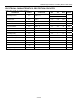
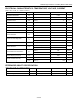
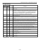
DC ELECTRICAL CHARACTERISTICS
(2.5V £ V
DD
£ 5.5V, T
A
= -20°C to +70°C.)
PARAMETER SYMBOL CONDITIONS MIN TYP MAX UNITS
Active Current I
ACTIVE
DQ = V
DD
, normal operation 60 90
mA
Sleep Mode Current I
SLEEP
DQ = 0V, no activity, PS floating
1 2
mA
Input Logic High: DQ, PIO V
IH
(Note 1) 1.5 V
Input Logic High: PS
V
IH
(Note 1) V
DD
- 0.2V V
Input Logic Low: DQ, PIO V
IL
(Note 1) 0.4 V
Input Logic Low: PS
V
IL
(Note 1) 0.2 V
Output Logic High: CC
V
OH
I
OH
= -0.1mA (Note 1) V
PLS
- 0.4V V
Output Logic High: DC
V
OH
I
OH
= -0.1mA (Note 1) V
DD
- 0.4V V
Output Logic Low: CC, DC
V
OL
I
OL
= 0.1mA (Note 1) 0.4 V
Output Logic Low: DQ, PIO V
OL
I
OL
= 4mA (Note 1) 0.4 V
DQ Pulldown Current I
PD
1
mA
Input Resistance: V
IN
R
IN
5
MW
Internal Current-Sense Resistor R
SNS
+25°C 20 25 30
mW
DQ Low to Sleep time t
SLEEP
2.1 s