
Datasheet


DS2762 High-Precision Li+ Battery Monitor With Alerts
9 of 25
POWER MODES
The DS2762 has two power modes: active and sleep. While in active mode, the DS2762 continually measures
current, voltage, and temperature to provide data to the host system and to support current accumulation and Li+
safety monitoring. In sleep mode, the DS2762 ceases these activities. The DS2762 enters sleep mode when any of
the following conditions occurs:
§ The PMOD bit in the Status Register has been set to 1 and the DQ line is low for longer than 2s (pack
disconnection).
§ The voltage on V
IN
drops below undervoltage threshold V
UV
for t
UVD
(cell depletion).
§ The pack is disabled through the issuance of a SWAP command (SWEN bit = 1).
The DS2762 returns to active mode when any of the following occurs:
§ The PMOD bit has been set to 1 and the SWEN bit is set to 0 and the DQ line is pulled high (pack
connection).
§ The
PS pin is pulled low (power switch).
§ The voltage on PLS becomes greater than the voltage on V
IN
(charger connection) with the SWEN bit set to 0.
§ The pack is enabled through the issuance of a SWAP command (SWEN bit = 1).
The DS2762 defaults to active mode when power is first applied.
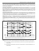
Li+ PROTECTION CIRCUITRY
During active mode, the DS2762 constantly monitors cell voltage and current to protect the battery from overcharge
(overvoltage), overdischarge (undervoltage), and excessive charge and discharge currents (overcurrent, short
circuit). Conditions and DS2762 responses are described in the following sections and summarized in Table 1 and
Figure 3.
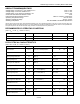
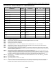
Table 1. Li+ Protection Conditions and DS2762 Responses
ACTIVATION
CONDITION
THRESHOLD DELAY RESPONSE
RELEASE THRESHOLD
Overvoltage V
IN
> V
OV
t
OVD
CC high
V
IN
< V
CE
, or
V
IS
≤ -2mV
Undervoltage V
IN
< V
UV
t
UVD
CC, DC high,
Sleep Mode
V
PLS
> V
DD
(1)
(charger connected)
Overcurrent, Charge V
IS
> V
OC
(2)
t
OCD
CC, DC high
V
PLS
< V
DD
- V
TP
(3)
Overcurrent, Discharge V
IS
< -V
OC
(2)
t
OCD
DC high
V
PLS
> V
DD
- V
TP
(4)
Short Circuit V
SNS
> V
SC
t
SCD
DC high
V
PLS
> V
DD
- V
TP
(4)
V
IS
= V
IS1
- V
IS2
. Logic high = V
PLS
for
CC
and V
DD
for
DC
.
All voltages are with respect to V
SS
. I
SNS
references current delivered from pin SNS.
Note 1:
If V
DD
< 2.2V, release is delayed until the recovery charge current (I
RC
) passed from PLS to V
DD
charges the battery and allows V
DD
to exceed 2.2V.
Note 2:
For the internal sense resistor configuration, the overcurrent thresholds are expressed in terms of current: I
SNS
> I
OC
for charge
direction and I
SNS
< -I
OC
for discharge direction.
Note 3:
With test current I
TST
flowing from PLS to V
SS
(pulldown on PLS).
Note 4:
With test current I
TST
flowing from V
DD
to PLS (pullup on PLS).
Overvoltage. If the cell voltage on V
IN
exceeds the overvoltage threshold, V
OV
, for a period longer than overvoltage
delay, t
OVD
, the DS2762 shuts off the external charge FET and sets the OV flag in the protection register. When the
cell voltage falls below charge enable threshold V
CE
, the DS2762 turns the charge FET back on (unless another
protection condition prevents it). Discharging remains enabled during overvoltage, and the DS2762 re-enables the
charge FET before V
IN
< V
CE
if a discharge current of -80mA (V
IS
≤ -2mV) or less is detected.
Undervoltage. If the voltage of the cell drops below undervoltage threshold, V
UV
, for a period longer than
undervoltage delay, t
UVD
, the DS2762 shuts off the charge and discharge FETs, sets the UV flag in the protection