
Datasheet


±5ppm, I
2
C Real-Time Clock
11Maxim Integrated
DS3231M
e.g., the microcontroller resets while reading data from
the device. When the microcontroller resets, the device’s
I
2
C interface can be placed into a known state by tog-
gling SCL until SDA is observed to be at a high level. At
that point the microcontroller should pull SDA low while
SCL is high, generating a START condition.
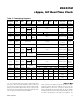
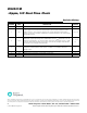
Address Map
Table 2 shows the address map for the device’s time-
keeping registers. During a multibyte access, when the
address pointer reaches the end of the register space
(12h), it wraps around to location 00h. On an I
2
C START
or address pointer incrementing to location 00h, the cur-
rent time is transferred to a second set of registers. The
Table 2. Timekeeping Registers
Note: Unless otherwise specified, the registers’ state is not defined when power is first applied.
ADDRESS
BIT 7
MSB
BIT 6 BIT 5 BIT 4 BIT 3 BIT 2 BIT 1
BIT 0
LSB
FUNCTION RANGE
00h 0 10 Seconds Seconds Seconds 00–59
01h 0 10 Minutes Minutes Minutes 00–59
02h 0
12/24
AM/PM
10
Hours
Hour Hours
1–12 +
AM/PM
00–23
20
Hours
03h 0 0 0 0 0 Day Day 1–7
04h 0 0 10 Date Date Date 01–31
05h Century 0 0
10
Month
Month Month/Century
01–12 +
Century
06h 10 Year Year Year 00–99
07h A1M1 10 Seconds Seconds
Alarm 1
Seconds
00–59
08h A1M2 10 Minutes Minutes
Alarm 1
Minutes
00–59
09h A1M3
12/24
AM/PM
10
Hours
Hour Alarm 1 Hours
1–12 +
AM/PM
00–23
20
Hours
0Ah A1M4
DY/DT
10 Date
Day Alarm 1 Day 1–7
Date Alarm 1 Date 1–31
0Bh A2M2 10 Minutes Minutes
Alarm 2
Minutes
00–59
0Ch A2M3
12/24
AM/PM
10
Hours
Hour Alarm 2 Hours
1–12 +
AM/PM
00–23
20
Hours
0Dh A2M4
DY/DT
10 Date
Day Alarm 2 Day 1–7
Date Alarm 2 Date 1–31
0Eh
EOSC
BBSQW CONV NA NA INTCN A2IE A1IE Control —
0Fh OSF 0 0 0 EN32KHZ BSY A2F A1F Status —
10h SIGN DATA DATA DATA DATA DATA DATA DATA Aging Offset 81h–7Fh
11h SIGN DATA DATA DATA DATA DATA DATA DATA
Temperature
MSB
—
12h DATA DATA 0 0 0 0 0 0
Temperature
LSB
—