
Datasheet


±5ppm, I
2
C Real-Time Clock
18 Maxim Integrated
DS3231M
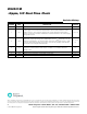
Manipulating the Address Counter for Reads: A
dummy write cycle can be used to force the address
counter to a particular value. To do this the mas-
ter generates a START condition, writes the slave
address byte (R/W = 0), writes the memory address
where it desires to read, generates a repeated START
condition, writes the slave address byte (R/W = 1),
reads data with ACK or NACK as applicable, and
generates a STOP condition. See Figure 6 for a read
example using the repeated START condition to
specify the starting memory location.
Reading Multiple Bytes from a Slave: The read
operation can be used to read multiple bytes with a
single transfer. When reading bytes from the slave,
the master simply ACKs the data byte if it desires to
read another byte before terminating the transaction.
After the master reads the last byte it must NACK to
indicate the end of the transfer and then it generates
a STOP condition.
Applications Information
Power-Supply Decoupling
To achieve the best results when using the DS3231M,
decouple the V
CC
and/or V
BAT
power supplies with
0.1FF and/or 1.0FF capacitors. Use a high-quality,
ceramic, surface-mount capacitor if possible. Surface-
mount components minimize lead inductance, which
improves performance, and ceramic capacitors tend to
have adequate high-frequency response for decoupling
applications.
If communications during battery operation are not
required, the V
BAT
decoupling capacitor can be omitted.
Using Open-Drain Outputs
The 32KHZ and INT/SQW outputs are open drain and
therefore require external pullup resistors to realize logic-
high output levels. Pullup resistor values between 1kI
and 10MI are typical.
The RST output is also open drain, but is provided with
an internal 50kI pullup resistor (R
PU
) to V
CC
. External
pullup resistors should not be added.
SDA and SCL Pullup Resistors
SDA is an open-drain output and requires an external
pullup resistor to realize a logic-high level.
Because the device does not use clock cycle stretching,
a master using either an open-drain output with a pullup
resistor or CMOS output driver (push-pull) could be used
for SCL.
Battery Charge Protection
The device contains Maxim Integrated’s redundant
battery-charge protection circuit to prevent any charging
of the external battery.
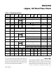
Figure 9. I
2
C Transactions
SLAVE
ADDRESS
START
START
1 1 0 1 0 0 0
SLAVE
ACK
SLAVE
ACK
SLAVE
ACK
R/W
MSB LSB MSB LSB MSB LSB
b7 b6 b5 b4 b3 b2 b1 b0
READ/
WRITE
REGISTER ADDRESS
b7 b6 b5 b4 b3 b2 b1 b0
DATA
STOP
SINGLE BYTE WRITE
-WRITE CONTROL REGISTER
TO 44h
MULTIBYTE WRITE
-WRITE DATE REGISTER
TO "02" AND MONTH
REGISTER TO "11"
SINGLE BYTE READ
-READ CONTROL REGISTER
MULTIBYTE READ
-READ ALARM 2 HOURS
AND DATE VALUES
START
REPEATED
START
D1h
MASTER
NACK
STOP1 1010000 00001110
0Eh
1 1010001
11010000 0 0001110
D0h 0Eh
STOP
VALUE
START 11010000 00000100
D0h 04h
DATA
MASTER
NACK
STOPVALUE
DATA
02h
44h
EXAMPLE I
2
C TRANSACTIONS
TYPICAL I
2
C WRITE TRANSACTION
01000100
00000010
D0h
A)
C)
B)
D)
SLAVE
ACK
SLAVE
ACK
SLAVE
ACK
SLAVE
ACK
SLAVE
ACK
SLAVE
ACK
SLAVE
ACK
REPEATED
START
D1h
MASTER
ACK
1 1010001 VALUE
DATA
SLAVE
ACK
SLAVE
ACK
SLAVE
ACK
START 11010000 00001100
D0h 0Ch
SLAVE
ACK
SLAVE
ACK
STOP
11h
00010001
SLAVE
ACK