
Instruction Manual


DS33R11 Ethernet Mapper with Integrated T1/E1/J1 Transceiver
161 of 344
11.5.3 Receive Serial Interface
Serial Receive Registers are used to control the HDLC Receiver associated with each Serial Interface. Note that
throughout this document HDLC Processor is also referred to as “Packet Processor”. The receive packet
processor block has seventeen registers.
11.5.3.1 Receive Serial Register Bit Descriptions
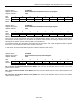
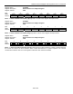
Register Name:
LI.RSLCR
Register Description:
Receive Serial Interface Configuration Register
Register Address:
100h
Bit # 7 6 5 4 3 2 1 0
Name - - - - - - - RDENPLT
Default 0 0 0 0 0 0 0 0
Bit 0: Receive Data Enable Polarity (RDENPLT) Receive Data Enable Polarity. If set to 1, RDEN Low enables
reception of the bit.
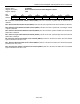
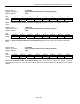
Register Name:
LI.RPPCL
Register Description:
Receive Packet Processor Control Low Register
Register Address:
101h
Bit # 7 6 5 4 3 2 1 0
Name - - RFPD RF16 RFED RDD RBRE RCCE
Default 0 0 0 0 0 0 0 0
Bit 5: Receive FCS Processing Disable (RFPD) – When equal to 0, FCS processing is performed and FCS is
appended to packets. When set to 1, FCS processing is disabled (the packets do not have an FCS appended). In
X.86 mode, FCS processing is always enabled.
Bit 4: Receive FCS-16 Enable (RF16) – When 0, the error checking circuit uses a 32-bit FCS. When 1, the error
checking circuit uses a 16-bit FCS. This bit is ignored when FCS processing is disabled. In X.86 mode, the FCS is
always 32 bits.
Bit 3: Receive FCS Extraction Disable (RFED) – When 0, the FCS bytes are discarded. When 1, the FCS bytes
are passed on. This bit is ignored when FCS processing is disabled. In X.86 mode, FCS bytes are discarded.
Bit 2: Receive Descrambling Disable (RDD) – When equal to 0, X
43
+1 descrambling is performed. When set to
1, descrambling is disabled.
Bit 1: Receive Bit Reordering Enable (RBRE) – When equal to 0, reordering is disabled and the first bit received
is expected to be the MSB DT [7] of the byte. When set to 1, bit reordering is enabled and the first bit received is
expected to be the LSB DT [0] of the byte.
Bit 0: Receive Clear Channel Enable (RCCE) – When equal to 0, packet processing is enabled. When set to 1,
the device is in clear channel mode and all packet-processing functions except descrambling and bit reordering are
disabled.