
Instruction Manual
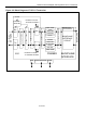

DS33R11 Ethernet Mapper with Integrated T1/E1/J1 Transceiver
29 of 344
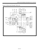
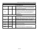
NAME PIN TYPE FUNCTION
PHY MANAGEMENT BUS
MDC C19 O
Management Data Clock (MII): Clocks management data between
the PHY and DS33R11. The clock is derived from theSYSCLKI,
with a maximum frequency is 1.67MHz. The user must leave this
pin unconnected in the DCE Mode.
MDIO C20 IO
MII Management data IO (MII): Data path for control information
between the PHY and DS33R11. When not used, pull to logic high
externally through a 10kΩ resistor. The MDC and MDIO pins are
used to write or read up to 32 Control and Status Registers in 32
PHY Controllers. This port can also be used to initiate Auto-
Negotiation for the PHY. The user must leave this pin unconnected
in the DCE Mode.
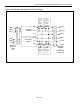
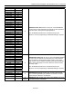
SDRAM INTERFACE
SCAS
W7 O
SDRAM Column Address Strobe: Active-low output, used to latch
the column address on the rising edge of SDCLKO. It is used with
commands for Bank Activate, Precharge, and Mode Register Write.
SRAS
W9 O
SDRAM Row Address Strobe: Active-low output, used to latch
the row address on rising edge of SDCLKO. It is used with
commands for Bank Activate, Precharge, and Mode Register Write.
SDCS
V10 O
SDRAM Chip Select: Active-low output enables SDRAM access.
SWE
W10 O
SDRAM Write Enable: This active-low output enables write
operation and auto precharge.
SBA[0] Y11
SBA[1] V11
O
SDRAM Bank Select: These 2 bits select 1 of 4 banks for the
read/write/precharge operations.
Note: All SDRAM operations are controlled entirely by the
DS33R11. No user programming for SDRAM buffering is required.