
Instruction Manual


DS33R11 Ethernet Mapper with Integrated T1/E1/J1 Transceiver
313 of 344
13 OPERATING PARAMETERS
ABSOLUTE MAXIMUM RATINGS
Voltage Range on Any Lead with Respect to V
SS
(except V
DD
)….………………………………………..-0.5V to +5.5V
Supply Voltage (VDD3.3) Range with Respect to V
SS
……………..……………………………………….-0.3V to +3.6V
Supply Voltage (VDD1.8) with Respect to V
SS
………………………..…….……………………………….-0.3V to +2.0V
Ambient Operating Temperature Range………………………………...………………………………......-40°C to +85°C
Junction Operating Temperature Range…………………………………...………………………………-40°C to +125°C
Storage Temperature Range……………………………………………………………………………..…-55°C to +125°C
Soldering Temperature………………………………………………………....See IPC/JEDEC J-STD-020 Specification
These are stress ratings only and functional operation of the device at these or any other conditions beyond those indicated in the operation
sections of this specification is not implied. Exposure to absolute maximum rating conditions for extended periods of time can affect reliability.
Ambient Operating Temperature Range is assuming the device is mounted on a JEDEC standard test board in a convection cooled JEDEC test
enclosure.
Note:
The “typ” values listed below are not production tested.
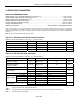
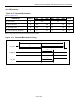
Table 13-1. Recommended DC Operating Conditions
(VDD3.3 = 3.3V ±5%, VDD1.8 = 1.8V ±5%, T
j
= -40°C to +85°C.)
PARAMETER SYMBOL CONDITIONS MIN TYP MAX UNITS
Logic 1 V
IH
2.35 3.465 V
Logic 0 V
IL
-0.3 +0.75 V
Supply (VDD3.3) ±5%
VDD3.3 3.135 3.300 3.465 V
Supply (VDD1.8) ±5% VDD1.8 1.71 1.8 1.89 V
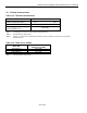
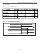
Table 13-2. DC Electrical Characteristics
(VDD3.3 = 3.3V ±5%, VDD1.8 = 1.8V ±5%, T
j
= -40°C to +85°C.)
PARAMETER SYMBOL CONDITIONS MIN TYP MAX UNITS
I/O Supply Current
(VDD3.3 = 3.465V)
I
DDIO
(Notes 1, 2)
100
mA
Core Supply Current
(VDD1.8 = 1.89V)
I
DDCORE
(Notes 1, 2)
30
mA
Lead Capacitance C
IO
(Note 3) 7 pF
I
IL
-10 +10
Input Leakage
I
ILP
-50 -10
μA
Output Leakage (when High-Z) I
LO
-10 +10
μA
(I
OH
= -4.0mA) V
OH
All outputs 2.35
(I
OL
= +4.0mA) V
OL
All outputs 0.75
(I
OH
= -8.0mA) V
OH
REF_CLKO 2.35
Output Voltage
(I
OL
= +12.0mA) V
OL
TSERO 0.75
V
V
IL
0.75
Input Voltage
V
IH
2.35
V
Note 1:
Typical power consumption is approximately 400mW.
Note 2:
All outputs loaded with rated capacitance; all inputs between V
DD
and V
SS
; inputs with pullups connected to V
DD
.
Note 3:
Value guaranteed by design (GBD).