
Instruction Manual

DS33R11 Ethernet Mapper with Integrated T1/E1/J1 Transceiver
32 of 344
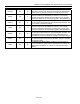
NAME PIN TYPE FUNCTION
TSIG B4 I
Transmit Signaling Input for the T1/E1/J1 Transceiver: When
enabled, this input will sample signaling bits for insertion into
outgoing PCM data stream. Sampled on the falling edge of TCLKT
when the transmit-side elastic store is disabled. Sampled on the
falling edge of TSYSCLK when the transmit-side elastic store is
enabled.
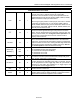
ETHERNET MAPPER TRANSMIT SERIAL INTERFACE
TSERO E2 O
Transmit Serial Data Output from Ethernet Mapper: Output on
the rising edge of TCLKE. Selective clock periods can be skipped
for output of TSERO with a gapped clock input on TCLKE. The
maximum data rate is 52Mbit/s.
TCLKE F1 I
Serial Interface Transmit Clock Input to Ethernet Mapper: The
clock reference for TSERO, which is output on the rising edge of
the clock. TCLKE supports gapped clocking, up to a maximum
frequency of 52MHz.
TDEN/
TBSYNC
D5 IO
Transmit Data Enable (Input): The transmit data enable is
programmable to selectively block/enable the transmit data. The
TDEN signal must occur one clock edge prior to the affected data
bit. The active polarity of TDEN is programmable in register
LI.TSLCR. It is recommended for both T1/E1 and T3/E3
applications that use gapped clocks. The TDEN signal is provided
for interfacing to framers that do not have a gapped clock facility.
Transmit Byte Sync (Output): This output can be used by an
external Serial to Parallel to convert TSERO stream to byte wide
data. This output indicates the last bit of the byte data sent serially
on TSERO. This signal is only active in the X.86 Mode.
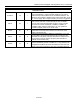
T1/E1/J1 RECEIVE FRAMER INTERFACE
RSERO H2 O
Receive Serial Data for T1/E1/J1 Transceiver: Received NRZ
serial data. Updated on rising edges of RCLKO when the receive-
side elastic store is disabled. Updated on the rising edges of
RSYSCLK when the receive-side elastic store is enabled.
RCLKO G3 O
Receive Clock Output from the T1/E1/J1 Framer: 1.544MHz (T1)
or 2.048MHz (E1) clock that is used to clock data through the
receive-side framer. Normally connected to the RCLKI input.
RCHBLK A1 O
Receive Channel Block for the T1/E1/J1 Transceiver: A user-
programmable output that can be forced high or low during any of
the 24 T1 or 32 E1 channels. Synchronous with RCLKO when the
receive-side elastic store is disabled. Synchronous with RSYSCLK
when the receive-side elastic store is enabled. Also useful for
locating individual channels in drop-and-insert applications, for
external per-channel loopback, and for per-channel conditioning.
See the Channel Blocking Registers section.
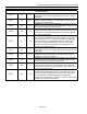
RCHCLK G2 O
Receive Channel Clock for the T1/E1/J1 Transceiver: A 192kHz
(T1) or 256kHz (E1) clock that pulses high during the LSB of each
channel can also be programmed to output a gated receive-bit
clock for fractional T1/E1 applications. Synchronous with RCLKO
when the receive-side elastic store is disabled. Synchronous with
RSYSCLK when the receive-side elastic store is enabled. Useful
for parallel-to-serial conversion of channel data.