
Instruction Manual

DS33R11 Ethernet Mapper with Integrated T1/E1/J1 Transceiver
37 of 344
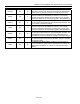
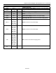
NAME PIN TYPE FUNCTION
SYSTEM CLOCKS
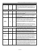
SYSCLKI V8 I
System Clock In for Ethernet Mapper: 100MHz System Clock
input to the DS33R11, used for internal operation. This clock is
buffered and provided at SDCLKO for the SDRAM interface. The
DS33R11 also provides a divided version output at the REF_CLKO
pin. A clock supply with ±100ppm frequency accuracy is suggested.
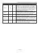
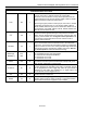
MCLK H4 I
Master Clock Input for the T1/E1/J1 Transceiver: A (50ppm)
clock source. This clock is used internally for both clock/data
recovery and for the jitter attenuator for both T1 and E1 modes.
The clock rate can be 16.384MHz, 8.192MHz, 4.096MHz, or
2.048MHz. When using the transceiver in T1-only operation a
1.544MHz (50ppm) clock source can be used.
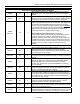
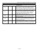
BPCLK B1 O
Backplane Clock from T1/E1/J1 Transceiver: A user-selectable
synthesized clock output that is referenced to the clock that is
output at the RCLKO pin.
8XCLK K4 O
Eight Times Clock from the T1/E1/J1 Transceiver: An 8x clock
that is locked to the recovered network clock provided from the
clock/data recovery block (if the jitter attenuator is enabled on the
receive side) or from the TDCLKI pin (if the jitter attenuator is
enabled on the transmit side).
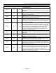
XTALD J4 O
Quartz Crystal Driver for the T1/E1/J1 Transceiver: A quartz
crystal of 2.048MHz (optional 1.544MHz in T1-only operation) can
be applied across MCLK and XTALD instead of a clock source at
MCLK. Leave open circuited if a clock source is applied at MCLK.