
Datasheet

V
DD
to GND .......................................................-0.3V to +3.97V
SCL, SDA, RST .................................................. -0.3V to +3.63V
All Other Pins to GND except
REG18 and REG274 ...........................-0.3V to (V
DD
+ 0.5V)*
Continous Sink Current ...................... 20mA per pin, 50mA total
Continous Source Current .................. 20mA per pin, 50mA total
Continuous Power Dissipation (T
A
= +70°C)
TQFN (derate 27.8mW/°C above + 70°C) .............2222.2mW
Operating Temperature Range ............................ -40ºC to +85ºC
Storage Temperature Range .............................-55ºC to +125ºC
Lead Temperature (soldering, 10s) ............................. …+300°C
Soldering Temperature (reflow) ................................... …+260°C
*Subject to not exceeding +3.97V.
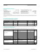
Recommended Operating Conditions
(T
A
= -40ºC to +85ºC, unless otherwise noted.) (Note 1)
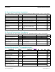
DC Electrical Characteristics
(V
DD
= 2.85V to 3.63V, T
A
= -40°C to +85°C, unless otherwise noted. Typical values are at V
DD
= 3.3V, T
A
= +25°C.) (Note 1)
PARAMETER SYMBOL CONDITIONS MIN TYP MAX UNITS
V
DD
Operating Voltage V
DD
(Note 2) 2.85 3.63 V
Input Logic-High V
IH
0.7 x
V
DD
V
DD
+
0.3
V
Input Logic-Low V
IL
-0.3
0.3 x
V
DD
V
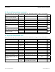
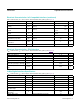
PARAMETER SYMBOL CONDITIONS MIN TYP MAX UNITS
Supply Current
I
CPU
CPU mode, all analog disabled
(Notes 3, 4)
7.25
mA
I
FASTCOMP
2.5
I
SAMPLEHOLDS
Both sample/hold 1.5
I
ADC
2.5
I
DACS
Per channel (Note 5) 0.7
Brownout Voltage V
BO
Monitors V
DD
(Note 2) 2.62 V
Brownout Hysteresis V
BOH
Monitors V
DD
(Note 2) 110 mV
1.8V Regulator Initial Voltage V
REG18
(Note 2) 1.71 1.8 1.89 V
2.74V Regulator Initial Voltage V
REG274
(Note 2) 2.68 2.74 2.80 V
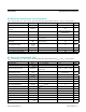
Clock Frequencies
f
OSC-
PERIPHERAL
T
A
= +25°C (Note 6) 20
MHz
f
MOSC-CORE
T
A
= +25°C (Note 6) 10
Clock Error f
ERR
T
A
= -40°C to +85°C 5 %
External Clock Input f
XCLK
20 133 MHz
DS4830A Optical Microcontroller
www.maximintegrated.com
Maxim Integrated
│
2
Absolute Maximum Ratings
Stresses beyond those listed under “Absolute Maximum Ratings” may cause permanent damage to the device. These are stress ratings only, and functional operation of the device at these
or any other conditions beyond those indicated in the operational sections of the specifications is not implied. Exposure to absolute maximum rating conditions for extended periods may affect
device reliability.