
Datasheet
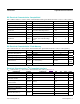
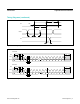

DC Electrical Characteristics: DAC
(V
DD
= 2.85V to 3.63V, T
A
= -40°C to +85°C unless otherwise noted. Typical values are at V
DD
= 3.3V, T
A
= +25°C.) (Note 1)
DC Electrical Characteristics (continued)
(V
DD
= 2.85V to 3.63V, T
A
= -40°C to +85°C, unless otherwise noted. Typical values are at V
DD
= 3.3V, T
A
= +25°C.) (Note 1)
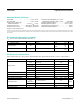
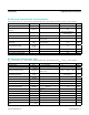
PARAMETER SYMBOL CONDITIONS MIN TYP MAX UNITS
Voltage Range: GP[15:0], SHEN,
DACPW[7:0], REFINA, REFINB
V
RANGE
(Note 2) -0.3
V
DD
+
0.3
V
Output Logic-Low: All Pins V
OL1
I
OL
= 4mA (Note 2) 0.4 V
Output Logic-High: All Pins Except
GP2, GP3, SCL, SDA
V
OH1
I
OH
= -4mA (Note 2)
V
DD
-
0.5
V
Pullup Current: All Pins Except GP2,
GP3, SCL, SDA
I
PU1
V
PIN
= 0V 55 µA
GPIO Drive Strength, Extra Strong
Outputs: GP0, GP1, MCS, PWM8,
PWM9
R
HISt
9 22
Ω
R
LOSt
8 22
GPIO Drive Strength, Strong
Outputs: MSDI, DACPW3, DACPW6
R
HIA
17 32
Ω
R
LOA
12 32
GPIO Drive Strength, Excluding
Strong GPIO Outputs
R
HIB
27 46
Ω
R
LOB
31 52
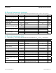
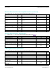
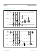
PARAMETER SYMBOL CONDITIONS MIN TYP MAX UNITS
DAC Resolution DAC
R
12 Bits
DAC Internal Reference Accuracy DAC
REFACC
(Note 5) -1.25 +1.25 %
DAC Internal Reference Power-Up
Speed
t
DACPUP
99% settled 10 µs
Reference Input Full-Scale Range
(REFINA, REFINB)
REFFS 1 2.5 V
DAC Operating Current I
DACS
Per channel
See the DC Electrical
Characteristics
mA
DAC Integral Nonlinearity DACINL (Note 5) 5 LSB
DAC Differential Nonlinearity DACDNL Not production tested (Notes 5, 7) ±1 LSB
DAC Offset V
OFFSET-DAC
At code “0” 0 18 mV
DAC Source Load Regulation I
DAC-SOURCE
0 to full-scale output, V
DD
= 3.3V 3 mV/mA
DAC Sink Capability and Sink Load
Regulation
R
DAC-SINK
0 to 0.5V output, limited by output
buffer impedance
500 Ω
I
DAC-SINK
0.5V to full-scale output 5 mV/mA
DAC Settling Time t
DAC
Output load capacitance between
33pF to 270pF, from 10% to 90%
10 µs
DS4830A Optical Microcontroller
www.maximintegrated.com
Maxim Integrated
│
3