
Datasheet
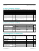
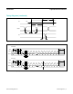

Electrical Characteristics: I
2
C-Compatible Interface (continued)
(V
DD
= 2.85V to 3.63V, T
A
= -40°C to +85°C, unless otherwise noted.) (Note 1) (See Figure 1.)
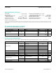
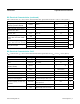
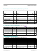
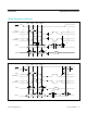
Electrical Characteristics: JTAG Interface
(V
DD
= 2.85V to 3.63V, T
A
= -40°C to +85°C, unless otherwise noted.) (Note 1) (See Figure 2.)
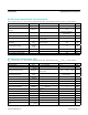
3-Wire Digital Interface Specication
(V
DD
= 2.85V to 3.63V, T
A
= -40°C to +85°C, unless otherwise noted.) (Note 1) (See Figure 3.)
PARAMETER SYMBOL CONDITIONS MIN TYP MAX UNITS
Data Setup Time t
SU:DAT
100 ns
SCL/MSCL, SDA/MSDA Capacitive
Loading
C
B
(Note 18) 400 pF
Rise Time of Both SDA and SCL
Signals
t
R
(Note 18)
20 +
0.1C
B
300 ns
Fall Time of Both SDA and SCL
Signals
t
F
(Note 18)
20 +
0.1C
B
300 ns
Setup Time for STOP Condition t
SU:STO
0.6 µs
Spike Pulse Width That Can Be
Suppressed by Input Filter
t
SP
(Note 19) 50 ns
SCL/MSCL and SDA/MSDA Input
Capacitance
C
BIN
5 pF
SMBusTimeout t
SMBUS
30 ms
PARAMETER SYMBOL CONDITIONS MIN TYP MAX UNITS
JTAG Logic Reference V
REF
V
DD
/2 V
TCK High Time t
TH
0.5 µs
TCK Low Time t
TL
0.5 µs
TCK Low to TDO Output t
TLQ
0.125 µs
TMS, TDI Input Setup to TCK High t
DVTH
0.25 µs
TMS, TDI Input Hold After TCK
High
t
THDX
0.25 µs
PARAMETER SYMBOL CONDITIONS MIN TYP MAX UNITS
MSCL Clock Frequency f
SCLOUT
1000 kHz
MSCL Duty Cycle t
3WDC
50 %
MSDIO Setup Time t
DS
100 ns
MSDIO Hold Time t
DH
100 ns
MCS Pulse-Width Low t
CSW
500 ns
MCS Leading Time Before the
First MSCL Edge
t
L
500 ns
MCS Trailing Time After the Last
MSCL Edge
t
T
500 ns
MSDIO, MSCL Load C
B3W
Total bus capacitance on one line 10 pF
DS4830A Optical Microcontroller
www.maximintegrated.com
Maxim Integrated
│
6