
Datasheet
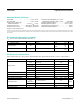
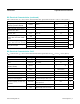
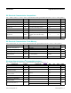
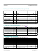
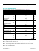

Note 10: Computed using end-point best fit and histogram method.
Note 11: ADC conversions are delayed up to 1.6µs if the fast comparator is sampling the selected ADC channel. This can cause a
slight decrease in the ADC sampling rate.
Note 12: Temperature readings averaged 64 times.
Note 13: Time from valid sample to ADC data available (without any averaging).
Note 14: Minimum and maximum timings depend upon f
MOSC-CORE
error.
Note 15: Programming does not include overhead associated with the utility ROM interface.
Note 16: f
SCL
must meet the minimum clock low time plus the rise/fall times.
Note 17: This device internally provides a hold time of at least 75ns for the SDA signal (referred to the V
IH:MIN
of the SCL signal) to
bridge the undefined region of the falling edge of SCL.
Note 18: C
B
—total capacitance of one bus line in pF.
Note 19: Filters on SDA and SCL suppress noise spikes at the input buffers and delay the sampling instant.
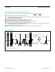
SPI Digital Interface Specication (continued)
(V
DD
= 2.85V to 3.63V, T
A
= -40°C to +85°C, unless otherwise noted.) (Note 1) (See Figure 4 and Figure 5.)
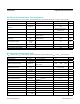
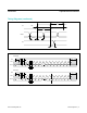
Figure 1. I
2
C Timing Diagram
SCL
NOTE: TIMING IS REFERENCED TO V
ILMAX
AND V
IHMIN
.
SDA
STOP STARTREPEATED
START
t
BUF
t
HD:STA
t
HD:DAT
t
SU:DAT
t
SU:STO
t
HD:STA
t
SP
t
SU:STA
t
HIGH
t
R
t
F
t
LOW
DS4830A Optical Microcontroller
www.maximintegrated.com
Maxim Integrated
│
8
Timing Diagrams