
Datasheet
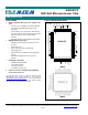


DS5001FP
4 of 27
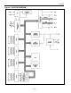
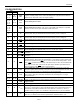
PIN DESCRIPTION
PIN
80 PIN 44 PIN
NAME FUNCTION
11, 9, 7,
5, 1, 79,
77, 75
31
(P0.5)
P0.0–
P0.7
General-Purpose I/O Port 0. This port is open-drain and cannot drive a logic 1. It
requires external pullups. Port 0 is also the multiplexed expanded address/data bus.
When used in this mode, it does not require pullups.
15, 17,
19, 21,
25, 27,
29, 31
44
(P1.3)
P1.0–
P1.7
General-Purpose I/O Port 1
49, 50,
51, 56,
58, 60,
64, 66
—
P2.0–
P2.7
General-Purpose I/O Port 2. Also serves as the MSB of the address in expanded
memory accesses, and as pins of the RPC mode when used.
36 8
P3.0/RX
D
General-Purpose I/O Port Pin 3.0. Also serves as the receive signal for the on
board UART. This pin should not be connected directly to a PC COM port.
38 10
P3.1/TX
D
General-Purpose I/O Port Pin 3.1. Also serves as the transmit signal for the on
board UART. This pin should not be connected directly to a PC COM port.
39 —
P3.2/
INT0
General-Purpose I/O Port Pin 3.2. Also serves as the active-low external interrupt
0.
40 11
P3.3/
INT1
General-Purpose I/O Port Pin 3.3. Also serves as the active-low external interrupt
1.
41 —
P3.4/T0
General-Purpose I/O Port Pin 3.4. Also serves as the timer 0 input.
44 12
P3.5/T1
General-Purpose I/O Port Pin 3.5. Also serves as the timer 1 input.
45 13
P3.6/
WR
General-Purpose I/O Port Pin. Also serves as the write strobe for expanded bus
operation.
46 —
P3.7/
RD
General-Purpose I/O Port Pin. Also serves as the read strobe for expanded bus
operation.
68 25
PSEN
Program Store Enable. This active-low signal is used to enable an external
program memory when using the expanded bus. It is normally an output and should
be unconnected if not used.
PSEN also is used to invoke the bootstrap loader. At this
time,
PSEN is pulled down externally. This should only be done once the DS5001FP
is already in a reset state. The device that pulls down should be open drain since it
must not interfere with
PSEN under normal operation.
34 6
RST
Active-High Reset Input. A logic 1 applied to this pin will activate a reset state.
This pin is pulled down internally so this pin can be left unconnected if not used. An
RC power-on reset circuit is not needed and is not recommended.
70 27
ALE
Address Latch Enable. Used to demultiplex the multiplexed expanded address/data
bus on port 0. This pin is normally connected to the clock input on a ’373 type
transparent latch.
47, 48 14, 15
XTAL2,
XTAL1
Crystal Connections. Used to connect an external crystal to the internal oscillator.
XTAL1 is the input to an inverting amplifier and XTAL2 is the output.
52 16
GND Logic Ground
13 39
V
CC
Power Supply, +5V
12 38
V
CCO
V
CC
Output. This is switched between V
CC
and V
LI
by internal circuits based on the
level of V
CC
. When power is above the lithium input, power will be drawn from V
CC
.
The lithium cell remains isolated from a load. When V
CC
is below V
LI
, the V
CCO
switches to the V
LI
source. V
CCO
should be connected to the V
CC
pin of an SRAM.
54 17
V
LI
Lithium Voltage Input. Connect to a lithium cell greater than V
LIMIN
and no greater
than V
LImax
as shown in the electrical specifications. Nominal value is +3V.