
Datasheet


DS5001FP
5 of 27
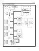
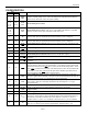
PIN DESCRIPTION (continued)
PIN
80 PIN 44 PIN
NAME FUNCTION
53, 16,
8, 18,
80, 76,
4, 6, 20,
24, 26,
28, 30,
33, 35,
37
41, 36,
42, 32,
30, 34,
35, 43,
1, 2, 3,
4, 5, 7,
9
BA14–
BA0
Byte-Wide Address Bus Bits 14–0. This bus is combined with the nonmultiplexed
data bus (BD7–0) to access NV SRAM. Decoding is performed using
CE1 through
CE4 . Therefore, BA15 is not actually needed. Read/write access is controlled by
R/
W . BA14–0 connect directly to an 8k, 32k, or 128k SRAM. If an 8k RAM is
used, BA13 and BA14 are unconnected. If a 128k SRAM is used, the micro converts
CE2 and CE3 to serve as A16 and A15 respectively.
71, 69,
67, 65,
61, 59,
57, 55
28, 26,
24, 23,
21, 20,
19, 18
BD7–0
Byte-Wide Data Bus Bits 7–0. This 8-bit, bidirectional bus is combined with the
nonmultiplexed address bus (BA14–0) to access NV SRAM. Decoding is performed
on
CE1 and CE2 . Read/write access is controlled by R/ W . BD7–0 connect directly to
an SRAM, and optionally to a real-time clock or other peripheral.
10 37
R/
W
Read/Write. This signal provides the write enable to the SRAMs on the byte-wide
bus. It is controlled by the memory map and partition. The blocks selected as
program (ROM) are write-protected.
74 29
CE1
Chip Enable 1. This is the primary decoded chip enable for memory access on the
byte-wide bus. It connects to the chip enable input of one SRAM. CE1 is lithium-
backed. It remains in a logic high inactive state when V
CC
falls below V
LI
.
72 —
CE1N
Non-Battery-Backed Version of Chip Enable 1. This can be used with a 32kB
EPROM. It should not be used with a battery-backed chip.
2 33
CE2
Chip Enable 2. This chip enable is provided to access a second 32k block of
memory. It connects to the chip enable input of one SRAM. When MSEL = 0, the
micro converts
CE2 into A16 for a 128k x 8 SRAM. CE2 is lithium-backed and
remains at a logic high when V
CC
falls below V
LI
.
63 22
CE3
Chip Enable 3. This chip enable is provided to access a third 32k block of memory.
It connects to the chip enable input of one SRAM. When MSEL = 0, the micro
converts
CE3 into A15 for a 128k x 8 SRAM. CE3 is lithium-backed and remains at
a logic high when V
CC
falls below V
LI
.
62 —
CE4
Chip Enable 4. This chip enable is provided to access a fourth 32k block of
memory. It connects to the chip-enable input of one SRAM. When MSEL = 0, this
signal is unused.
CE4 is lithium-backed and remains at a logic high when V
CC
< V
LI
.
78 —
PE1
Peripheral Enable 1. Accesses data memory between addresses 0000h and 3FFFh
when the PES bit is set to a logic 1. Commonly used to chip enable a byte-wide real-
time clock such as the DS1283.
PE1 is lithium-backed and remains at a logic high
when V
CC
falls below V
LI
. Connect PE1 to battery-backed functions only.
3 —
PE2
Peripheral Enable 2. Accesses data memory between addresses 4000h and 7FFFh
when the PES bit is set to a logic 1.
PE2 is lithium-backed and remains at a logic
high when V
CC
falls below V
LI
. Connect PE2 to battery-backed functions only.
22 —
PE3
Peripheral Enable 3. Accesses data memory between addresses 8000h and BFFFh
when the PES bit is set to a logic 1.
PE3 is not lithium-backed and can be connected
to any type of peripheral function. If connected to a battery-backed chip, it needs
additional circuitry to maintain the chip enable in an inactive state when V
CC
< V
LI
.
23 —
PE4
Peripheral Enable 4. Accesses data memory between addresses C000h and FFFFh
when the PES bit is set to a logic 1.
PE4 is not lithium-backed and can be connected
to any type of peripheral function. If connected to a battery-backed chip, it needs
additional circuitry to maintain the chip enable in an inactive state when V
CC
< V
LI
.
32 —
PROG
Invokes the bootstrap loader on a falling edge. This signal should be debounced
so that only one edge is detected. If connected to ground, the micro enters bootstrap
loading on power-up. This signal is pulled up internally.