
Datasheet


DS80C320/DS80C323 High-Speed/Low-Power Microcontrollers
22 of 38
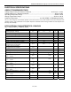
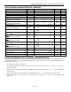
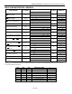
NOTES FOR DS80C320 DC ELECTRICAL CHARACTERISTICS
All parameters apply to both commercial and industrial temperature operation unless otherwise noted. Specifications to -40°C
are guaranteed by design and are not production tested.
1. All voltages are referenced to ground.
2. Active current is measured with a 25MHz clock source driving XTAL1, V
CC
= RST = 5.5V, all other pins
disconnected.
3. Idle mode current is measured with a 25MHz clock source driving XTAL1, V
CC
= 5.5V, RST at ground, all
other pins disconnected.
4. Stop mode current measured with XTAL1 and RST grounded, V
CC
= 5.5V, all other pins disconnected.
5. When addressing external memory. This specification only applies to the first clock cycle following transition.
6. RST = V
CC
. This condition mimics operation of pins in I/O mode.
7. During a 0-to-1 transition, a one-shot drives the ports hard for two clock cycles. This measurement reflects port
in transition mode.
8. Ports 1 and 3 source transition current when being pulled down externally. It reaches its maximum at
approximately 2V.
9. 0.45<V
IN
<V
CC
. Not a high-impedance input. This port is a weak address holding latch because Port 0 is
dedicated as an address bus on the DS80C320. Peak current occurs near the input transition point of the latch,
approximately 2V.
10. Over the industrial temperature range, this specification has a maximum value of 200A.
11. This is the current required from an external circuit to hold a logic low level on an I/O pin while the
corresponding port latch bit is set to 1. This is only the current required to hold the low level; transitions from 1
to 0 on an I/O pin will also have to overcome the transition current.
12. Device operating range is 4.5V to 5.5V; however, device is tested to 4.0V to ensure proper operation at
minimum V
RST
.
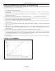
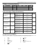
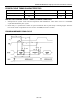
TYPICAL I
CC
vs. FREQUENCY