DS80C320/DS80C323 High-Speed/Low-Power Microcontrollers www.maxim-ic.
DS80C320/DS80C323 High-Speed/Low-Power Microcontrollers DETAILED DESCRIPTION The DS80C320/DS80C323 are fast 80C31/80C32-compatible microcontrollers. Wasted clock and memory cycles have been removed using a redesigned processor core. As a result, every 8051 instruction is executed between 1.5 and 3 times faster than the original for the same crystal speed. Typical applications see a speed improvement of 2.5 times using the same code and same crystal.
DS80C320/DS80C323 High-Speed/Low-Power Microcontrollers Figure 1. Block Diagram DS80C320/ DS80C323 PIN DESCRIPTION PIN NAME FUNCTION DIP PLCC TQFP 40 44 38 VCC +5V (+3V for DS80C323) 20 22, 23 16, 17 GND Digital Circuit Ground Reset Input. The RST input pin contains a Schmitt voltage input to recognize external active-high reset inputs. The pin also employs an internal pulldown resistor to allow for a combination of wired OR external reset sources.
DS80C320/DS80C323 High-Speed/Low-Power Microcontrollers PIN DESCRIPTION (continued) PIN DIP PLCC TQFP NAME FUNCTION 30 33 27 ALE Address Latch-Enable Output. This pin functions as a clock to latch the external address LSB from the multiplexed address/data bus. This signal is commonly connected to the latch enable of an external 373 family transparent latch. ALE has a pulse width of 1.5 XTAL1 cycles and a period of four XTAL1 cycles. ALE is forced high when the device is in a reset condition.
DS80C320/DS80C323 High-Speed/Low-Power Microcontrollers PIN DESCRIPTION (continued) DIP 21 22 23 24 25 26 27 PIN PLCC 24 25 26 27 28 29 30 TQFP 18 19 20 21 22 23 24 NAME FUNCTION A8 (P2.0) A9 (P2.1) A10 (P2.2) A11 (P2.3) A12 (P2.4) A13 (P2.5) A14 (P2.6) 28 31 25 A15 (P2.7) Port 2, Output. Port 2 serves as the MSB for external addressing. P2.7 is A15 and P2.0 is A8. The device will automatically place the MSB of an address on P2 for external ROM and RAM access.
DS80C320/DS80C323 High-Speed/Low-Power Microcontrollers 80C32 COMPATIBILITY The DS80C320/DS80C323 are CMOS 80C32-compatible microcontrollers designed for high performance. In most cases, the devices will drop into an existing 80C32 design to significantly improve the operation. Every effort has been made to keep the devices familiar to 8032 users, yet they have many new features. In general, software written for existing 80C32-based systems will work on the DS80C320 and DS80C323.
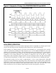
DS80C320/DS80C323 High-Speed/Low-Power Microcontrollers Figure 2. Comparative Timing of the DS80C320/DS80C323 and 80C32 DS80C320/DS80C323 TIMING STANDARD 80C32 TIMING HIGH-SPEED OPERATION The DS80C320/DS80C323 are built around a high-speed, 80C32-compatible core. Higher speed comes not just from increasing the clock frequency but also from a newer, more efficient design. In this updated core, dummy memory cycles have been eliminated.
DS80C320/DS80C323 High-Speed/Low-Power Microcontrollers INSTRUCTION SET SUMMARY All instructions in the DS80C320/DS80C323 perform the same functions as their 80C32 counterparts. Their effect on bits, flags, and other status functions is identical. However, the timing of each instruction is different. This applies both in absolute and relative number of clocks. For absolute timing of real-time events, the timing of software loops will need to be calculated using the Table 1.
DS80C320/DS80C323 High-Speed/Low-Power Microcontrollers Table 1.
DS80C320/DS80C323 High-Speed/Low-Power Microcontrollers Table 1.
DS80C320/DS80C323 High-Speed/Low-Power Microcontrollers Table 1 shows the speed for each class of instruction. Note that many of the instructions have multiple op codes. There are 255 op codes for 111 instructions. Of the 255 op codes, 159 are three times faster than the original 80C32. While a system that emphasizes those instructions will see the most improvement, the large total number that receive a 3 to 1 improvement assure a dramatic speed increase for any system.
DS80C320/DS80C323 High-Speed/Low-Power Microcontrollers STRETCH MEMORY CYCLE The DS80C320/DS80C323 allow the application software to adjust the speed of data memory access. The microcontroller is capable of performing the MOVX in as little as two instruction cycles. However, this value can be stretched as needed so that both fast memory and slow memory or peripherals can be accessed with no glue logic.
DS80C320/DS80C323 High-Speed/Low-Power Microcontrollers DUAL DATA POINTER Data memory block moves can be accelerated using the Dual Data Pointer (DPTR). The standard 8032 DPTR is a 16-bit value that is used to address off-chip data RAM or peripherals. In the DS80C320/DS80C323, the standard 16-bit data pointer is called DPTR0 and is located at SFR addresses 82h and 83h. These are the standard locations. The new DPTR is located at SFR 84h and 85h and is called DPTR1.
DS80C320/DS80C323 High-Speed/Low-Power Microcontrollers 64-Byte Block Move with Dual Data Pointer ; SH and SL are high and low byte source address. ; DH and DL are high and low byte of destination address. ; DPS is the data pointer select. Reset condition is DPS=0, DPTR0 is selected.
DS80C320/DS80C323 High-Speed/Low-Power Microcontrollers POWER-FAIL RESET The DS80C320/DS80C323 incorporate a precision bandgap voltage reference to determine when VCC is out of tolerance. While powering up, internal circuits will hold the device in a reset state until VCC rises above the VRST reset threshold. Once VCC is above this level, the oscillator will begin running. An internal reset circuit will then count 65,536 clocks to allow time for power and the oscillator to stabilize.
DS80C320/DS80C323 High-Speed/Low-Power Microcontrollers a 25MHz crystal frequency. Note that once the counter chain has reached a conclusion, the optional interrupt is generated. Regardless of whether the user enables this interrupt, there are then 512 clocks left until a reset occurs. There are 5 control bits in special function registers that affect the Watchdog Timer and two status flags that report to the user. The Reset Watchdog Timer bit (WDCON.
DS80C320/DS80C323 High-Speed/Low-Power Microcontrollers POWER MANAGEMENT The DS80C320/DS80C323 provide the standard Idle and power-down (Stop) modes that are available on the standard 80C32. However, the device has enhancements that make these modes more useful, and allow more power saving. The Idle mode is invoked by setting the LSB of the Power Control register (PCON to 87h). Idle will leave internal clocks, serial port and timer running.
DS80C320/DS80C323 High-Speed/Low-Power Microcontrollers immediately preceding the setting of the Stop bit to guarantee a correct power-on delay when exiting Stop mode. The second feature allows an additional power saving option. This is the ability to start instantly when exiting Stop mode. It is accomplished using an internal ring oscillator that can be used when exiting Stop mode in response to an interrupt. The benefit of the ring oscillator is as follows.
DS80C320/DS80C323 High-Speed/Low-Power Microcontrollers Figure 4. Ring Oscillator Startup DIAGRAM ASSUMES THAT THE OPERATION FOLLOWING STOP REQUIRES LESS THAN 18ms COMPLETE. TIMED ACCESS PROTECTION Selected SFR bits are critical to operation, making it desirable to protect against an accidental write operation. The Timed Access procedure prevents an errant CPU from accidentally altering a bit that would cause difficulty.
DS80C320/DS80C323 High-Speed/Low-Power Microcontrollers SPECIAL-FUNCTION REGISTERS Most special features of the DS80C320/DS80C323 or 80C32 are controlled by bits in the SFRs, allowing the devices to add many features but use the same instruction set. When writing software to use a new feature, the SFR must be defined to an assembler or compiler using an equate statement. This is the only change needed to access the new function.
DS80C320/DS80C323 High-Speed/Low-Power Microcontrollers ELECTRICAL SPECIFICATIONS ABSOLUTE MAXIMUM RATINGS Voltage Range on Any Pin Relative to Ground…………………………………………-0.3V to (VCC + 0.5V) Voltage Range on VCC Relative to Ground……………………………………………………..-0.3V to +6.0V Operating Temperature Range………………………………………………………………….-40°C to +85°C Storage Temperature Range…………………………………………………………………..-55°C to +125°C Soldering Temperature…………………………………………….
DS80C320/DS80C323 High-Speed/Low-Power Microcontrollers NOTES FOR DS80C320 DC ELECTRICAL CHARACTERISTICS All parameters apply to both commercial and industrial temperature operation unless otherwise noted. Specifications to -40°C are guaranteed by design and are not production tested. 1. All voltages are referenced to ground. 2. Active current is measured with a 25MHz clock source driving XTAL1, VCC = RST = 5.5V, all other pins disconnected. 3.
DS80C320/DS80C323 High-Speed/Low-Power Microcontrollers AC CHARACTERISTICS—DS80C320 PARAMETER Oscillator Frequency External Oscillator External Crystal ALE Pulse Width Port 0 Address Valid to ALE Low Address Hold After ALE Low Address Hold After ALE Low for MOVX WR ALE Low to Valid Instruction In ALE Low to PSEN Low PSEN Pulse Width PSEN Low to Valid Instruction In Input Instruction Hold After PSEN Input Instruction Float After PSEN Port 0 Address to Valid Instruction In Port 2 Address to Valid Instru
DS80C320/DS80C323 High-Speed/Low-Power Microcontrollers MOVX CHARACTERISTICS—DS80C320 PARAMETER SYMBOL RD Pulse Width tRLRH WR Pulse Width tWLWH RD Low to Valid Data In tRLDV Data Hold After Read tRHDX Data Float After Read tRHDZ ALE Low to Valid Data In tLLDV Port 0 Address to Valid Data In Port 2 Address to Valid Data In VARIABLE CLOCK MIN 2tCLCL-11 tMCS-11 2tCLCL-11 tMCS-11 tLLWL Port 0 Address Valid to RD or WR Low tAVWL1 Port 2 Address Valid to RD or WR Low tAVWL2 Data Valid to WR
DS80C320/DS80C323 High-Speed/Low-Power Microcontrollers DC ELECTRICAL CHARACTERISTICS—DS80C323 PARAMETER Operating Supply Voltage Power-Fail Warning Voltage Minimum Operating Voltage Supply Current Active Mode at 18MHz Supply Current Idle Mode at 18MHz Supply Current Stop Mode, Bandgap Reference Disabled Supply Current Stop Mode, Bandgap Reference Enabled Input Low Level Input High Level (Except XTAL1 and RST) Input High Level XTAL1 and RST Output Low Voltage Ports 1, 3 at IOL = 1.
DS80C320/DS80C323 High-Speed/Low-Power Microcontrollers NOTES FOR DS80C323 DC ELECTRICAL CHARACTERISTICS (continued) All parameters apply to both commercial and industrial temperature operation unless otherwise noted. Specifications to -40°C are guaranteed by design and are not production tested. Device operating range is 2.7V to 5.5V. DC electrical specifications are for operation 2.7V to 3.3V. 6. RST = VCC. This condition mimics operation of pins in I/O mode. 7.
DS80C320/DS80C323 High-Speed/Low-Power Microcontrollers AC ELECTRICAL CHARACTERISTICS—DS80C323 PARAMETER Oscillator Frequency External Oscillator External Crystal ALE Pulse Width Port 0 Address Valid to ALE Low Address Hold After ALE Low Address Hold After ALE Low for MOVX WR ALE Low to Valid Instruction In ALE Low to PSEN Low PSEN Pulse Width PSEN Low to Valid Instruction In Input Instruction Hold After PSEN Input Instruction Float After PSEN Port 0 Address to Valid Instruction In Port 2 Address to V
DS80C320/DS80C323 High-Speed/Low-Power Microcontrollers MOVX CHARACTERISTICS—DS80C323 PARAMETER SYMBOL RD Pulse Width tRLRH WR Pulse Width tWLWH RD Low to Valid Data In tRLDV Data Hold After Read tRHDX Data Float After Read tRHDZ ALE Low to Valid Data In tLLDV Port 0 Address to Valid Data In Port 2 Address to Valid Data In VARIABLE CLOCK MIN 2tCLCL-11 tMCS-11 2tCLCL-11 tMCS-11 Port 0 Address Valid to RD or WR Low tAVWL1 Port 2 Address Valid to RD or WR Low tAVWL2 Data Valid to WR Transi
DS80C320/DS80C323 High-Speed/Low-Power Microcontrollers EXTERNAL CLOCK CHARACTERISTICS PARAMETER Clock High Time Clock Low Time Clock Rise Time Clock Fall Time SYMBOL tCHCX tCLCX tCLCH tCHCL MIN 10 10 TYP MAX 5 5 UNITS ns ns ns ns SERIAL PORT MODE 0 TIMING CHARACTERISTICS PARAMETER Serial Port Clock Cycle Time Output Data Setup to Clock Rising Edge Output Data Hold from Clock Rising Input Data Hold After Clock Rising Clock Rising Edge to Input Data Valid SYMBOL tXLXL tQVXH tXHQX tXHDX tXHDV
DS80C320/DS80C323 High-Speed/Low-Power Microcontrollers POWER-CYCLE TIMING CHARACTERISTICS PARAMETER SYMBOL Crystal Startup Time tCSU Power-On Reset Delay tPOR MIN TYP MAX 1.8 65,536 UNITS NOTES ms 1 tCLCL 2 NOTES FOR POWER CYCLE TIMING CHARACTERISTICS 1. Startup time for crystals varies with load capacitance and manufacturer. Time shown is for an 11.0592MHz crystal manufactured by Fox crystal. 2. Reset delay is a synchronous counter of crystal oscillations after crystal startup.
DS80C320/DS80C323 High-Speed/Low-Power Microcontrollers DATA MEMORY READ CYCLE 31 of 38
DS80C320/DS80C323 High-Speed/Low-Power Microcontrollers DATA MEMORY WRITE CYCLE DATA MEMORY WRITE WITH STRETCH = 1 32 of 38
DS80C320/DS80C323 High-Speed/Low-Power Microcontrollers DATA MEMORY WRITE WITH STRETCH = 2 4-CYCLE DATA MEMORY WRITE STRETCH VALUE = 2 EXTERNAL CLOCK DRIVE 33 of 38
DS80C320/DS80C323 High-Speed/Low-Power Microcontrollers SERIAL PORT MODE 0 TIMING SERIAL PORT 0 (SYNCHRONOUS MODE) HIGH SPEED OPERATION SM2 = 1 ≥ TXD CLOCK = XTAL/4 SERIAL PORT 0 (SYNCHRONOUS MODE) SM2 = 0 ≥ TXD CLOCK = XTAL/12 34 of 38
DS80C320/DS80C323 High-Speed/Low-Power Microcontrollers POWER-CYCLE TIMING 35 of 38
DS80C320/DS80C323 High-Speed/Low-Power Microcontrollers PACKAGE INFORMATION For the latest package outline information and land patterns, go to www.maxim-ic.com/packages. PACKAGE TYPE PACKAGE CODE DOCUMENT NO.
DS80C320/DS80C323 High-Speed/Low-Power Microcontrollers DATA SHEET REVISION SUMMARY The following represent the key differences between the 101006 and 070505 version of the DS80C320/DS80C323 data sheet. Please review this summary carefully. 1. Deleted DS80C323-MND from Ordering Information table (page 2). Device was never manufactured. The following represent the key differences between the 070505 and 051804 version of the DS80C320/DS80C323 data sheet. Please review this summary carefully. 2.
DS80C320/DS80C323 High-Speed/Low-Power Microcontrollers DATA SHEET REVISION SUMMARY (continued) The following represent the key differences between the 05/22/96 and the 10/21/97 version of the DS80C320 data sheet. Please review this summary carefully. DS80C320 1. Added note to clarify IIL specification. 2. Added note to clarify AC timing conditions. 3. Corrected erroneous tQVXL label on figure “Serial Port Mode 0 Timing” to read tQVXH. 4.