
Datasheet


DS80C320/DS80C323 High-Speed/Low-Power Microcontrollers
4 of 38
PIN DESCRIPTION (continued)
PIN
DIP PLCC
TQFP
NAME FUNCTION
30 33 27 ALE
Address Latch-Enable Output. This pin functions as a clock to latch
the external address LSB from the multiplexed address/data bus. This
signal is commonly connected to the latch enable of an external 373
family transparent latch. ALE has a pulse width of 1.5 XTAL1 cycles
and a period of four XTAL1 cycles. ALE is forced high when the
device is in a reset condition.
39 43 37 AD0
38 42 36 AD1
37 41 35 AD2
36 40 34 AD3
35 39 33 AD4
34 38 32 AD5
33 37 31 AD6
32 36 30 AD7
Port 0, Input/Output. Port 0 is the multiplexed address/data bus.
During the time when ALE is high, the LSB of a memory address is
presented. When ALE falls, the port transitions to a bidirectional data
bus. This bus is used to read external ROM and read/write external
RAM memory or peripherals. The Port 0 has no true port latch and
cannot be written directly by software. The reset condition of Port 0 is
high. No pullup resistors are needed.
Port 1, I/O. Port 1 functions as both an 8-bit, bidirectional I/O port and
an alternate functional interface for Timer 2 I/O, new External
Interrupts, and new Serial Port 1. The reset condition of Port 1 is with
all bits at logic 1. In this state, a weak pullup holds the port high. This
condition also serves as an input mode, since any external circuit that
writes to the port will overcome the weak pullup. When software writes
a 0 to any port pin, the device will activate a strong pulldown that
remains on until either a 1 is written or a reset occurs. Writing a 1 after
the port has been at 0 will cause a strong transition driver to turn on,
followed by a weaker sustaining pullup. Once the momentary strong
driver turns off, the port once again becomes the output high (and
input) state. The alternate modes of Port 1 are outlined as follows:
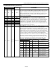
PIN
DIP PLCC TQFP
PORT ALTERNATE FUNCTION
1 2 40
P1.0 T2
External I/O for
Timer/Counter 2
2 3 41
P1.1 T2EX
Timer/Counter 2
Capture/Reload Trigger
3 4 42
P1.2 RXD1 Serial Port 1 Input
4 5 43
P1.3 TXD1 Serial Port 1 Output
5 6 44
P1.4 INT2
External Interrupt 2
(Positive-Edge Detect)
6 7 1
P1.5
INT3
External Interrupt 3
(Negative-Edge Detect)
7 8 2
P1.6 INT4
External Interrupt 4
(Positive-Edge Detect)
1–8 2–9
40–44,
1–3
P1.0–P1.7
8 9 3
P1.7
INT5
External Interrupt 5
(Negative-Edge Detect)