
Datasheet


DS80C320/DS80C323 High-Speed/Low-Power Microcontrollers
5 of 38
PIN DESCRIPTION (continued)
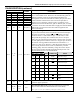
PIN
DIP PLCC TQFP
NAME FUNCTION
21 24 18 A8 (P2.0)
22 25 19 A9 (P2.1)
23 26 20 A10 (P2.2)
24 27 21 A11 (P2.3)
25 28 22 A12 (P2.4)
26 29 23 A13 (P2.5)
27 30 24 A14 (P2.6)
28 31 25 A15 (P2.7)
Port 2, Output. Port 2 serves as the MSB for external addressing.
P2.7 is A15 and P2.0 is A8. The device will automatically place the
MSB of an address on P2 for external ROM and RAM access.
Although Port 2 can be accessed like an ordinary I/O port, the value
stored on the Port 2 latch will never be seen on the pins (due to
memory access). Therefore, writing to Port 2 in software is only
useful for the instructions MOVX A, @Ri or MOVX @Ri, A. These
instructions use the Port 2 internal latch to supply the external address
MSB. In this case, the Port 2 latch value will be supplied as the
address information.
Port 3, Input/Output. Port 3 functions as both an 8-bit, bidirectional
I/O port and an alternate functional interface for External Interrupts,
Serial Port 0, Timer 0 & 1 Inputs,
RD
and WR strobes. The reset
condition of Port 3 is with all bits at logic 1. In this state, a weak
pullup holds the port high. This condition also serves as an input
mode, since any external circuit that writes to the port will overcome
the weak pullup. When software writes a 0 to any port pin, the device
will activate a strong pulldown that remains on until either a 1 is
written or a reset occurs. Writing a 1 after the port has been at 0 will
cause a strong transition driver to turn on, followed by a weaker
sustaining pullup. Once the momentary strong driver turns off, the
port once again becomes both the output high and input state. The
alternate modes of Port 3 are outlined below:
PIN
DIP PLCC TQFP
PORT ALTERNATE MODE
10 11 5 P3.0 RXD0 Serial Port 0 Input
11 13 7 P3.1 TXD0 Serial Port 0 Output
12 14 8 P3.2
INT0
External Interrupt 0
13 15 9 P3.3
INT1
External Interrupt 1
14 16 10 P3.4 T0 Timer 0 External Input
15 17 11 P3.5 T1 Timer 1 External Input
16 18 12 P3.6
WR
External Data Memory Write
Strobe
10–17
11, 13–
19
5, 7–13 P3.0–P3.7
17 19 13 P3.7
RD
External Data Memory Read
Strobe
31 35 29
EA
External Access, Active-Low Input. This pin must be connected to
ground for proper operation.
—
12, 34,
1*
6, 28,
39*
N.C.
No Connection (Reserved). These pins should not be connected.
They are reserved for use with future devices in this family.
*These pins are reserved for additional ground pins on future products.