
Datasheet


DS80C320/DS80C323 High-Speed/Low-Power Microcontrollers
3 of 38
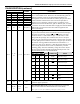
Figure 1. Block Diagram
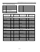
PIN DESCRIPTION
PIN
DIP PLCC
TQFP
NAME FUNCTION
40 44
38 V
CC
+5V (+3V for DS80C323)
20 22, 23
16, 17 GND
Digital Circuit Ground
9 10 4 RST
Reset Input. The RST input pin contains a Schmitt voltage input to
recognize external active-high reset inputs. The pin also employs an
internal pulldown resistor to allow for a combination of wired OR
external reset sources. An RC is not required for power-up, as the device
provides this function internally.
18 20 14 XTAL2
19 21 15 XTAL1
Crystal Oscillator Pins. XTAL1 and XTAL2 provide support for
parallel-resonant, AT-cut crystals. XTAL1 acts also as an input in the
event that an external clock source is used in place of a crystal. XTAL2
serves as the output of the crystal amplifier.
29 32 26
PSEN
Program Store-Enable Output, Active Low. This signal is commonly
connected to external ROM memory as a chip enable.
PSEN provides an
active-low pulse width of 2.25 XTAL1 cycles with a period of four
XTAL1 cycles.
PSEN is driven high when data memory (RAM) is being
accessed through the bus and during a reset condition.
DS80C320/
DS80C323