www. maxi mi nt egr at ed.
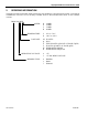
High-Speed Microcontroller User’s Guide TABLE OF CONTENTS 1. 2. 3. INTRODUCTION..............................................................................................................9 ORDERING INFORMATION..........................................................................................10 ARCHITECTURE...........................................................................................................11 3.1 3.2 ALU........................................................................
High-Speed Microcontroller User’s Guide 4.2.26 4.2.27 4.2.28 4.2.29 4.2.30 4.2.31 4.2.32 4.2.33 4.2.34 4.2.35 4.2.36 4.2.37 4.2.38 4.2.39 4.2.40 4.2.41 4.2.42 4.2.43 4.2.44 4.2.45 4.2.46 4.2.47 4.2.48 4.2.49 4.2.50 4.2.51 4.2.52 4.2.53 4.2.54 4.2.55 4.2.56 4.2.57 4.3 4.4 INSTRUCTION TIMING .....................................................................................................................58 ADDRESSING MODES...................................................................................
High-Speed Microcontroller User’s Guide 6. MEMORY ACCESS .......................................................................................................76 6.1 6.2 INTERNAL PROGRAM MEMORY .......................................................................................................76 INTERNAL DATA MEMORY ..............................................................................................................76 6.2.1 6.3 6.4 6.5 ROMSIZE Feature .....................................
High-Speed Microcontroller User’s Guide 10.2 PORT 2.................................................................................................................................... 113 10.2.1 10.2.2 10.3 10.4 10.5 10.6 10.7 10.8 10.9 10.10 11. General-Purpose I/O .......................................................................................................................... 113 Most Significant Address Byte, A8–A15 ..........................................................................
High-Speed Microcontroller User’s Guide 12.5 12.6 13. 13.1 13.2 13.3 14. 14.1 14.2 14.3 14.4 14.5 14.6 15. 15.1 15.2 16. 17. 17.1 17.2 17.3 17.4 17.5 17.6 18. 18.1 18.2 18.3 18.4 19. FRAMING ERROR DETECTION ...................................................................................................149 MULTIPROCESSOR COMMUNICATION ........................................................................................151 TIMED-ACCESS PROTECTION ................................................
High-Speed Microcontroller User’s Guide LIST OF FIGURES Figure 4-1. Memory Map .......................................................................................................................... 15 Figure 4-2. Register Map.......................................................................................................................... 16 Figure 4-3. Scratchpad Register Addressing............................................................................................ 16 Figure 5-1.
High-Speed Microcontroller User’s Guide LIST OF TABLES Table 4-A. DS80C310 SFR Locations...................................................................................................... 17 Table 4-B. DS80C310 SFR Reset Values ................................................................................................ 18 Table 4-C. DS80C320/DS80C323 SFR Locations ...................................................................................19 Table 4-D. DS80C320/DS80C323 SFR Reset Values .....
High-Speed Microcontroller User’s Guide 1. INTRODUCTION Maxim high-speed microcontrollers are 8051-compatible devices that provide improved performance and power consumption compared to the original version. They retain instruction-set and object-code compatibility with the 8051, yet perform the same operations in fewer clock cycles. Consequently, more throughput is possible for the same crystal speed.
High-Speed Microcontroller User’s Guide 2. ORDERING INFORMATION The high-speed microcontroller family follows the part numbering convention shown below. Note that all combinations of devices are not currently available. Refer to the individual data sheets for the available versions.
High-Speed Microcontroller User’s Guide 3. ARCHITECTURE The high-speed microcontroller is based on the industry-standard 80C52. The core is an accumulatorbased architecture using internal registers for data storage and peripheral control. It executes the standard 8051 instruction set. This section provides a brief description of each architecture feature. Details concerning the programming model, instruction set, and register description are provided in Section 4. 3.
High-Speed Microcontroller User’s Guide 3.2.7 Timer/Counters Three 16-bit Timer/Counters are available in the high-speed microcontroller. Each timer is contained in two SFR locations that can be written or read by software. The timers are controlled by other SFRs described in Section 4. 3.2.8 UARTs The high-speed microcontroller provides one or two UARTs. These are controlled and accessed as SFRs. Each UART has an address that is used to read or write the UART.
High-Speed Microcontroller User’s Guide monitor invokes a reset condition. This remains until power returns to normal operating voltage. The power monitor also functions on power-up, holding the microcontroller in a reset state until power is stable. 3.2.16 Interrupts The high-speed microcontroller is capable of evaluating a number of interrupt sources simultaneously. Each version of the high-speed microcontroller provides a different number of interrupt sources.
High-Speed Microcontroller User’s Guide 4. PROGRAMMING MODEL This section provides a programmer’s overview of the high-speed microcontroller core. It includes information on the memory map, on-chip RAM, SFRs, and instruction set. The programming model of the high-speed microcontroller is very similar to that of the industry standard 80C52. The memory map is identical. It uses the same instruction set, though instruction timing is improved. Several new SFRs have been added. 4.
High-Speed Microcontroller User’s Guide SFRs are accessed directly between 80h and FFh (128 to 255). The RAM locations between 128 and 255 can be reached through an indirect reference to those locations. Scratchpad RAM is available for general-purpose data storage. It is commonly used in place of off-chip RAM when the total data contents are small. When off-chip RAM is needed, the Scratchpad area still provides the fastest general-purpose access.
High-Speed Microcontroller User’s Guide Figure 4-2. Register Map FFh 255 FFh INDIRECT RAM DIRECT SFRs 128 7Fh 0000h 7Fh DIRECT RAM Figure 4-3.
High-Speed Microcontroller User’s Guide 4.2 Special Function Registers The high-speed microcontroller, like the 8051, uses special function registers (SFRs) to control peripherals and modes. In many cases, an SFR will control individual functions or report status on individual functions. The SFRs reside in register locations 80h–FFh and are reached using direct addressing. SFRs that end in 0 or 8 are bit addressable.
High-Speed Microcontroller User’s Guide Table 4-B.
High-Speed Microcontroller User’s Guide Table 4-C. DS80C320/DS80C323 SFR Locations REGISTER SP DPL DPH DPL1 DPH1 DPS PCON TCON TMOD TL0 TL1 TH0 TH1 CKCON P1 EXIF SCON0 SBUF0 P2 IE SADDR0 SADDR1 P3 IP SADEN0 SADEN1 SCON1 SBUF1 STATUS TA T2CON T2MOD RCAP2L RCAP2H TL2 TH2 PSW WDCON ACC EIE B EIP BIT 7 BIT 6 BIT 5 BIT 4 BIT 3 BIT 2 BIT 1 BIT 0 SP.7 SP.6 SP.5 SP.4 SP.3 SP.2 SP.1 SP.0 DPL.7 DPL.6 DPL.5 DPL.4 DPL.3 DPL.2 DPL.1 DPL.0 DPH.7 DPH.6 DPH.5 DPH.4 DPH.3 DPH.2 DPH.1 DPH.0 DPL1.7 DPL1.6 DPL1.5 DPL1.
High-Speed Microcontroller User’s Guide Table 4-D.
High-Speed Microcontroller User’s Guide Table 4-E. DS83C520/DS87C520 SFR Locations REGISTER P0 SP DPL DPH DPL1 DPH1 DPS PCON TCON TMOD TL0 TL1 TH0 TH1 CKCON P1 EXIF SCON0 SBUF0 P2 IE SADDR0 SADDR1 P3 IP SADEN0 SADEN1 SCON1 SBUF1 ROMSIZE PMR STATUS TA T2CON T2MOD RCAP2L RCAP2H TL2 TH2 PSW WDCON ACC EIE B EIP BIT 7 P0.7 SP.7 DPL.7 DPH.7 DPL1.7 DPH1.7 0 SMOD_0 TF1 GATE TL0.7 TL1.7 TH0.7 TH1.7 WD1 P1.7 IE5 SM0/FE_0 SBUF0.7 P2.7 EA SADDR0.7 SADDR1.7 P3.7 — SADEN0.7 SADEN1.7 SM0/FE_1 SBUF1.7 — CD1 PIP TA.
High-Speed Microcontroller User’s Guide Table 4-F.
High-Speed Microcontroller User’s Guide Table 4-G. DS87C530 SFR Locations REGISTER P0 SP DPL DPH DPL1 DPH1 DPS PCON TCON TMOD TL0 TL1 TH0 TH1 CKCON P1 EXIF TRIM SCON0 SBUF0 P2 IE SADDR0 SADDR1 P3 IP SADEN0 SADEN1 SCON1 SBUF1 ROMSIZE PMR STATUS TA T2CON T2MOD RCAP2L RCAP2H TL2 TH2 PSW WDCON ACC EIE B RTASS RTAS RTAM RTAH EIP RTCC RTCSS Rev: 062210 BIT 7 P0.7 SP.7 DPL.7 DPH.7 DPL1.7 DPH1.7 0 SMOD_0 TF1 GATE TL0.7 TL1.7 TH0.7 TH1.7 WD1 P1.7 IE5 E4K SM0/FE_0 SBUF0.7 P2.7 EA SADDR0.7 SADDR1.7 P3.7 — SADEN0.
High-Speed Microcontroller User’s Guide REGISTER RTCS RTCM RTCH RTCD0 RTCD1 BIT 7 0 0 DOW.2 RTCD0.7 RTCD1.7 BIT 6 0 0 DOW.1 RTCD0.6 RTCD1.6 BIT 5 RTCS.5 RTCM.5 DOW.0 RTCD0.5 RTCD1.5 BIT 4 RTCS.4 RTCM.4 RTCH.4 RTCD0.4 RTCD1.4 BIT 3 RTCS.3 RTCM.3 RTCH.3 RTCD0.3 RTCD1.3 BIT 2 RTCS.2 RTCM.2 RTCH.2 RTCD0.2 RTCD1.2 BIT 1 RTCS.1 RTCM.1 RTCH.1 RTCD0.1 RTCD1.1 BIT 0 RTCS.0 RTCM.0 RTCH.0 RTCD0.0 RTCD1.
High-Speed Microcontroller User’s Guide REGISTER B RTASS RTAS RTAM RTAH EIP RTCC RTCSS RTCS RTCM RTCH RTCD0 RTCD1 BIT 7 0 SPECIAL 0 0 0 — SPECIAL SPECIAL 0 0 SPECIAL SPECIAL SPECIAL BIT 6 0 SPECIAL 0 0 0 — SPECIAL SPECIAL 0 0 SPECIAL SPECIAL SPECIAL BIT 5 0 SPECIAL SPECIAL SPECIAL 0 0 SPECIAL SPECIAL SPECIAL SPECIAL SPECIAL SPECIAL SPECIAL BIT 4 0 SPECIAL SPECIAL SPECIAL SPECIAL 0 SPECIAL SPECIAL SPECIAL SPECIAL SPECIAL SPECIAL SPECIAL BIT 3 0 SPECIAL SPECIAL SPECIAL SPECIAL 0 0 SPECIAL SPECIAL SPECIAL
High-Speed Microcontroller User’s Guide 4.2.3 Data Pointer Low 0 (DPL) SFR 82h 7 6 5 4 3 2 1 0 DPL.7 DPL.6 DPL.5 DPL.4 DPL.3 DPL.2 DPL.1 DPL.0 RW-0 RW-0 RW-0 RW-0 RW-0 RW-0 RW-0 RW-0 R = Unrestricted Read, W = Unrestricted Write, -n = Value after Reset Data Pointer Low 0. This register is the low byte of the standard 80C32 16-bit data pointer. DPL and DPH are used to point to non-scratchpad data RAM. DPL.7–DPL.0 Bits 7–0 4.2.
High-Speed Microcontroller User’s Guide 4.2.7 Data Pointer Select (DPS) SFR 86h 7 6 5 4 3 2 1 0 0 0 0 0 0 0 0 SEL R-0 R-0 R-0 R-0 R-0 R-0 R-0 RW-0 R = Unrestricted Read, W = Unrestricted Write, -n = Value after Reset Bits 7-1 Reserved. These bits will read 0. SEL Bit 0 Data Pointer Select. This bit selects the active data pointer. 0 = Instructions that use the DPTR will use DPL and DPH. 1 = Instructions that use the DPTR will use DPL1 and DPH1. 4.2.
High-Speed Microcontroller User’s Guide 4.2.9 Timer/Counter Control (TCON) SFR 88h 7 6 5 4 3 2 1 0 TF1 TR1 TF0 TR0 IE1 IT1 IE0 IT0 RW-0 RW-0 RW-0 RW-0 RW-0 RW-0 RW-0 RW-0 R = Unrestricted Read, W = Unrestricted Write, -n = Value after Reset TF1 Bit 7 TR1 Bit 6 TF0 Bit 5 TR0 Bit 4 IE1 Bit 3 Timer 1 Overflow Flag. This bit indicates when Timer 1 overflows its maximum count as defined by the current mode.
High-Speed Microcontroller User’s Guide 4.2.10 SFR 89h Timer Mode Control (TMOD) 7 6 5 4 3 2 1 0 GATE C/ T M1 M0 GATE C/ T M1 M0 RW-0 RW-0 RW-0 RW-0 RW-0 RW-0 RW-0 RW-0 R = Unrestricted Read, W = Unrestricted Write, -n = Value after Reset GATE Bit 7 C/T Bit 6 Timer 1 Gate Control. This bit enable/disables the ability of Timer 1 to increment. 0 = Timer 1 will clock when TR1 = 1, regardless of the state of INT1. 1 = Timer 1 will clock only when TR1 = 1 and INT1 = 1.
High-Speed Microcontroller User’s Guide 4.2.11 Timer 0 LSB (TL0) SFR 8Ah 7 6 5 4 3 2 1 0 TL0.7 TL0.6 TL0.5 TL0.4 TL0.3 TL0.2 TL0.1 TL0.0 RW-0 RW-0 RW-0 RW-0 RW-0 RW-0 RW-0 RW-0 R = Unrestricted Read, W = Unrestricted Write, -n = Value after Reset Timer 0 LSB. This register contains the least significant byte of Timer 0. TL0.7–TL0.0 Bits 7–0 4.2.12 Timer 1 LSB (TL1) SFR 8Bh 7 6 5 4 3 2 1 0 TL1.7 TL1.6 TL1.5 TL1.4 TL1.3 TL1.2 TL1.1 TL1.
High-Speed Microcontroller User’s Guide 4.2.15 SFR 8Eh Clock Control (CKCON) 7 6 5 4 3 2 1 0 WD1 WD0 T2M T1M T0M MD2 MD1 MD0 RW-0 RW-0 RW-0 RW-0 RW-0 RW-0 RW-0 RW-1 R = Unrestricted Read, W = Unrestricted Write, -n = Value after Reset WD1, WD0 Bits 7, 6 Watchdog Timer Mode Select 1-0. These bits determine the watchdog timer timeout period. The timer divides the crystal frequency by a programmable value as shown below. The divider value is expressed in clock (crystal) cycles.
High-Speed Microcontroller User’s Guide 4.2.16 SFR 90h Port 1 (P1) 7 6 4 3 2 1 0 P1.6 5 P1.5 P1.7 INT5 P1.4 P1.3 P1.2 P1.1 P1.0 INT4 INT3 INT2 TXD1 RXD1 T2EX T2 RW-1 RW-1 RW-1 RW-1 RW-1 RW-1 RW-1 RW-1 R = Unrestricted Read, W = Unrestricted Write, -n = Value after Reset P1.7–P1.0 Bits 7–0 INT5 Bit 7 General-Purpose I/O Port 1. This register functions as a general purpose I/O port. In addition, all the pins have an alternative function listed below. P1.
High-Speed Microcontroller User’s Guide 4.2.17 SFR 91h External Interrupt Flag (EXIF) 7 6 5 4 3 2 1 0 IE5 IE4 IE3 IE2 XT/ RG RGMD RGSL BGS RW-0 RW-0 RW-0 RW-0 RW-* R-* RW-* RT-0 R = Unrestricted Read, W = Unrestricted Write, T = Timed Access Write Only-n = Value after Reset, * = See description IE5 Bit 7 External Interrupt 5 Flag. This bit will be set when a falling edge is detected on INT5 . This bit must be cleared manually by software.
High-Speed Microcontroller User’s Guide Bandgap Select. This bit enables/disables the bandgap reference during Stop mode. Disabling the bandgap reference provides significant power savings in Stop mode, but sacrifices the ability to perform a power-fail interrupt or power-fail reset while stopped. This bit can only be modified with a Timed Access procedure. The state of this bit will be undefined on devices that do not incorporate a bandgap reference.
High-Speed Microcontroller User’s Guide 4.2.19 Serial Port 0 Control (SCON0) SFR 98h 7 6 5 4 3 2 1 0 SM0/FE_0 SM1_0 SM2_0 REN_0 TB8_0 RB8_0 TI_0 RI_0 RW-0 RW-0 RW-0 RW-0 RW-0 RW-0 RW-0 RW-0 R = Unrestricted Read, W = Unrestricted Write, -n = Value after Reset Serial Port Mode. These bits control the mode of serial port 0. In addition the SM0 and SM2_0 bits have secondary functions as shown below.
High-Speed Microcontroller User’s Guide TI_0 Bit 1 Transmitter Interrupt Flag. This bit indicates that data in the serial port 0 buffer has been completely shifted out. In serial port mode 0, TI_0 is set at the end of the 8th data bit. In all other modes, this bit is set at the end of the last data bit. This bit must be manually cleared by software. RI_0 Bit 0 Receiver Interrupt Flag. This bit indicates that a byte of data has been received in the serial port 0 buffer.
High-Speed Microcontroller User’s Guide 4.2.22 Interrupt Enable (IE) SFR A8h 7 6 5 4 3 2 1 0 EA ES1 ET2 ES0 ET1 EX1 ET0 EX0 RW-0 RW-0 RW-0 RW-0 RW-0 RW-0 RW-0 RW-0 R = Unrestricted Read, W = Unrestricted Write, -n = Value after Reset Global Interrupt Enable. This bit controls the global masking of all interrupts except power-fail interrupt, which is enabled by the EPFI bit (WDCON.5). 0 = Disable all interrupt sources. This bit overrides individual interrupt mask settings.
High-Speed Microcontroller User’s Guide 4.2.24 SFR AAh Slave Address Register 1 (SADDR1) 7 6 5 4 3 2 1 0 SADDR1.7 SADDR1.6 SADDR1.5 SADDR1.4 SADDR1.3 SADDR1.2 SADDR1.1 SADDR1.0 RW-0 RW-0 RW-0 RW-0 RW-0 RW-0 RW-0 RW-0 R = Unrestricted Read, W = Unrestricted Write, -n = Value after Reset Slave Address Register 1. This register is programmed with the given or broadcast address assigned to serial port 1. SADDR1.7– SADDR1.0 Bits 7–0 4.2.
High-Speed Microcontroller User’s Guide 4.2.26 Interrupt Priority (IP) SFR B8h 7 6 5 4 3 2 1 0 — PS1 PT2 PS0 PT1 PX1 PT0 PX0 — RW-0 RW-0 RW-0 RW-0 RW-0 RW-0 RW-0 R = Unrestricted Read, W = Unrestricted Write, -n = Value after Reset Bit 7 PS1 Bit 6 Reserved. Read data is indeterminate. Serial Port 1 Interrupt. This bit controls the priority of the serial port 1 interrupt. 0 = Serial port 1 priority is determined by the natural priority order.
High-Speed Microcontroller User’s Guide 4.2.28 Slave Address Mask Enable Register 1 (SADEN1) 7 SFR BAh SADEN1.7 6 5 4 3 2 1 0 SADEN1.6 SADEN1.5 SADEN1.4 SADEN1.3 SADEN1.2 SADEN1.1 SADEN1.0 RW-0 RW-0 RW-0 RW-0 RW-0 RW-0 RW-0 RW-0 R = Unrestricted Read, W = Unrestricted Write, -n = Value after Reset Slave Address Mask Enable Register 1. This register functions as a mask when comparing serial port 1 addresses for automatic address recognition.
High-Speed Microcontroller User’s Guide Multiple CPU Communications. The function of this bit is dependent on the serial port 1 mode. Mode 0: Selects 12tCLK or 4tCLK period for synchronous port 1 data transfers. Mode 1: When this bit is set, reception is ignored (RI_1) is not set) if invalid stop bit received. Mode 2/3: when this bit is set, multiprocessor communications are enabled in mode 2 and 3. This will prevent RI_1 from being set, and an interrupt being asserted, if the 9th bit received is not 1.
High-Speed Microcontroller User’s Guide 4.2.31 ROM Size Select (ROMSIZE) SFR C2h 7 6 5 4 3 2 1 0 — — — — — RMS2 RMS1 RMS0 RT-1 RT-0 RT-1 R = Unrestricted Read, W = Unrestricted Write, -n = Value after Reset Bits 7–3 RMS2, RMS1, RMS0 Bits 2, 1, 0 These bits are reserved. Read data is indeterminate. ROM Size Select 2-0. This register is used to select the maximum on-chip decoded address for ROM.
High-Speed Microcontroller User’s Guide 4.2.32 Power Management Register (PMR) SFR C4h 7 6 5 4 3 2 1 0 CD1 CD0 SWB — XTOFF ALEOFF DME1 DME0 RW-0 RW-1 RW-0 RW*-0 RW-0 RW-0 RW-0 R = Unrestricted Read, W = Unrestricted Write, -n = Value after Reset, * = See description Clock Divide Control 1-0. These bits select the number of crystal oscillator clocks required to generate one machine cycle. Switching between modes requires a transition through the divide-by-4 mode (CD1, CD0 = 01).
High-Speed Microcontroller User’s Guide Data Memory Enable 1-0. These bits determine the functional relationship of the first 1024 bytes of data memory. Three memory configurations are supported to allow either external data memory access through the expanded multiplexed address/data bus of Ports 0 and Port 2, internal SRAM data memory access, or read-only access to EPROM programming information.
High-Speed Microcontroller User’s Guide 4.2.33 SFR C5h Status Register (STATUS) 7 6 5 4 3 2 1 0 PIP HIP LIP XTUP SPTA1 SPRA1 SPTA0 SPRA0 R-0 R-0 R-0 R-0* R-0 R-0 R-0 R-0 R = Unrestricted Read, W = Unrestricted Write, -n = Value after Reset, * = See description PIP Bit 7 Power-Fail Priority Interrupt Status. When set, this bit indicates that software is currently servicing a power-fail interrupt. It is cleared when the program executes the corresponding RETI instruction.
High-Speed Microcontroller User’s Guide 4.2.34 SFR C7h Timed Access Register (TA) 7 6 5 4 3 2 1 0 TA.7 TA.6 TA.5 TA.4 TA.3 TA.2 TA.1 TA.0 W-1 W-1 W-1 W-1 W-1 W-1 W-1 W-1 W = Unrestricted Write, -n = Value after Reset Timed Access. Correctly accessing this register permits modification of timed-access protected bits. Write AAh to this register first, followed within 3 cycles by writing 55h.
High-Speed Microcontroller User’s Guide Timer 2 External Enable. This bit enables the capture/ reload function on the T2EX pin if Timer 2 is not generating baud rates for the serial port. 0 = Timer 2 will ignore all external events at T2EX. 1 = Timer 2 will capture or reload a value if a negative transition is detected on the T2EX pin. Timer 2 Run Control. This bit enables/disables the operation of timer 2. Halting this timer will preserve the current count in TH2, TL2. 0 = Timer 2 is halted.
High-Speed Microcontroller User’s Guide 4.2.37 SFR CAh Timer 2 Capture LSB (RCAP2L) 7 6 5 4 3 2 1 0 RCAP2L.7 RCAP2L.6 RCAP2L.5 RCAP2L.4 RCAP2L.3 RCAP2L.2 RCAP2L.1 RCAP2L.0 RW-0 RW-0 RW-0 RW-0 RW-0 RW-0 RW-0 RW-0 R = Unrestricted Read, W = Unrestricted Write, -n = Value after Reset Timer 2 Capture LSB. This register is used to capture the TL2 value when timer 2 is configured in capture mode.
High-Speed Microcontroller User’s Guide 4.2.41 SFR D0h Program Status Word (PSW) 7 6 5 4 3 2 1 0 CY AC F0 RS1 RS0 OV F1 P RW-0 RW-0 RW-0 RW-0 RW-0 RW-0 RW-0 RW-0 R = Unrestricted Read, W = Unrestricted Write, -n = Value after Reset CY Bit 7 Carry Flag. This bit is set when if the last arithmetic operation resulted in a carry (during addition) or a borrow (during subtraction). Otherwise it is cleared to 0 by all arithmetic operations. AC Bit 6 Auxiliary Carry Flag.
High-Speed Microcontroller User’s Guide 4.2.42 SFR D8h Watchdog Control (WDCON) 7 6 5 4 3 2 1 0 SMOD POR EPFI PFI WDIF WTRF EWT RWT RW-0 RT-* RW-0 RW-* RT-0 RT-* RT-* RT-0 R = Unrestricted Read, W = Unrestricted Write, T = Timed Access Write Only, -n = Value after Reset, * = See Description Serial Modification. This bit controls the doubling of the serial port 1 baud rate in modes 1, 2, and 3.
High-Speed Microcontroller User’s Guide Enable Watchdog Timer Reset. This bit enables/disables the ability of the watchdog timer to reset the device. This bit has no effect on the ability of the watchdog timer to generate a watchdog interrupt. The watchdog timer mode select bits (CKCON.7-6) control the timeout period of the watchdog timer.
High-Speed Microcontroller User’s Guide 4.2.44 SFR E8h Extended Interrupt Enable (EIE) 7 6 5 4 3 2 1 0 — — ERTCI EWDI EX5 EX4 EX3 EX2 RW-0 RW-0 RW-0 RW-0 RW-0 RW-0 R = Unrestricted Read, W = Unrestricted Write, -n = Value after Reset Bits 7, 6 ERTCI Bit 5 Reserved. Read data will be indeterminate. Real-Time Clock Interrupt Enable. This bit enables/disables the real-time clock interrupt on the DS87C530. This bit will read 0 on all other devices.
High-Speed Microcontroller User’s Guide 4.2.47 SFR F3h Real-Time Alarm Second Register (RTAS) 7 6 5 4 3 2 1 0 0 0 RTAS.5 RTAS.4 RTAS.3 RTAS.2 RTAS.1 RTAS.0 RW-0 RW-0 RW-* RW-* RW-* RW-* RW-* RW-* R = Unrestricted Read, W = Unrestricted Write, -n = Value after Reset, * = See description Bits 7, 6 RTAS.5–RTAS.0 Bits 5–0 4.2.48 SFR F4h Reserved. These bits will be 0 when read. Real-Time Alarm Second.
High-Speed Microcontroller User’s Guide 4.2.50 SFR F8h Extended Interrupt Priority (EIP) 7 6 5 4 3 2 1 0 — — PRTCI PWDI PX5 PX4 PX3 PX2 RW-0 RW-0 RW-0 RW-0 RW-0 RW-0 R = Unrestricted Read, W = Unrestricted Write, -n = Value after Reset Bits 7, 6 PRTCI Bit 5 PWDI Bit 4 PX5 Bit 3 PX4 Bit 2 PX3 Bit 1 PX2 Bit 0 Rev: 062210 Reserved. These bits will be 0 when read. Real-Time Clock Interrupt Priority. This bit controls the priority of the real–time clock interrupt on the DS87C530.
High-Speed Microcontroller User’s Guide 4.2.51 SFR F9h Real-Time Clock Control Register (RTCC) 7 6 5 4 3 2 1 0 SSCE SCE MCE HCE RTCRE RTCWE RTCIF RTCE RW-* RW-* RW-* RW-* RW*-0 RT*-0 R*-* RT-* R = Unrestricted Read, W = Unrestricted Write, T = Timed Access Write Only, -n = Value after Reset, * = See Description SSCE Bit 7 SCE Bit 6 MCE Bit 5 HCE Bit 4 RTCRE Bit 3 Rev: 062210 RTC Subsecond Register Compare Enable.
High-Speed Microcontroller User’s Guide 1 = Reads of the RTC clock registers are permitted during a 1 ms window starting from the time the bit is set. Immediately after setting this bit, software must wait 4 machine cycles to allow all time registers to synchronize. The user should clear this bit when the desired reads are complete, although it will clear automatically within 1.95ms if not cleared in software. RTC Write Enable.
High-Speed Microcontroller User’s Guide 4.2.53 SFR FBh Real-Time Clock Second Register (RTCS) 7 6 5 4 3 2 1 0 0 0 RTCS.5 RTCS.4 RTCS.3 RTCS.2 RTCS.1 RTCS.0 R*-0 R*-0 R*W*-* R*W*-* R*W*-* R*W*-* R*W*-* R*W*-* R = Unrestricted Read, W = Unrestricted Write, -n = Value after Reset, * = See Description Bits 7, 6 Reserved. These bits will be 0 when read. RTCS.5–RTCS.0 Bits 5–0 Real-Time Clock Seconds. This register represents the second value of the RTC.
High-Speed Microcontroller User’s Guide 4.2.56 SFR FEh Real-Time Clock Day Register 0 (RTCD0) 7 6 5 4 3 2 1 0 RTCD0.7 RTCD0.6 RTCD0.5 RTCD0.4 RTCD0.3 RTCD0.2 RTCD0.1 RTCD0.0 R*W*-* R*W*-* R*W*-* R*W*-* R*W*-* R*W*-* R*W*-* R*W*-* R = Unrestricted Read, W = Unrestricted Write, -n = Value after Reset, * = See Description RTCD0.7–RTCD.0 Bits 7-0 4.2.57 SFR FFh Real-Time Clock Day Register 0. This register contains the least significant byte of the 16-bit current day count.
High-Speed Microcontroller User’s Guide 4.4 Addressing Modes The high-speed microcontroller uses the standard 8051 instruction set, which a wide range of third-party assemblers and compilers supports. Like the 8051, the high-speed microcontroller uses three memory areas. These are program memory, data memory, and registers. Both the program and data areas are 64kB each. They extend from 0000h to FFFFh.
High-Speed Microcontroller User’s Guide 4.4.2 Direct Addressing Direct Addressing is the mode used to access the entire lower 128 bytes of Scratchpad RAM and the SFR area. It is commonly used to move the value in one register to another. Two examples are shown below. MOV 72h, 74h MOV 90h, 20h ;Move the value in register 74 to ;register 72. ;Move the value in register 20 to ;the SFR at 90h (Port 1) Note that there is no instruction difference between a RAM access and an SFR access.
High-Speed Microcontroller User’s Guide The 16-bit Data pointers (DPTRs) can be used as an absolute off-chip reference. This gives access to the entire 64kB data memory map. An example is as follows. MOVX @DPTR, A ;Write the value in the accumulator ;to the address referenced by the ;selected data pointer. 4.4.4 Immediate Addressing Immediate Addressing is used when one of the operands is predetermined and coded into the software.
High-Speed Microcontroller User’s Guide 4.4.8 Extended Addressing Extended Addressing is used by the Branching instructions to specify a 16-bit destination address within the 64kB address space. The destination address is fixed in software as an absolute value. An example is as follows. LJMP 4.5 0F732h ;Jump to address 0F732h. Program Status Flags All program status flags are contained in the program status word at SFR location D0h.
High-Speed Microcontroller User’s Guide 5. CPU TIMING The timing of the high-speed microcontroller is the area with the greatest departure from the original 8051 series. This section will briefly explain the timing and also compare it to the original. 5.1 Oscillator The high-speed microcontroller provides an on-chip oscillator circuit that can be driven by an external crystal or by an off-chip TTL clock source.
High-Speed Microcontroller User’s Guide Figure 5-1. Crystal Connection HIGH-SPEED MICROCONTROLLER XTAL1 TO INTERNAL CIRCUITS XTAL2 33pF 33pF Figure 5-2. Clock Source Input HIGH-SPEED MICRO CLOCK OSCILLATOR XTAL1 TO INTERNAL CIRCUITS XTAL2 5.6 Instruction Timing The clock source, whether crystal or oscillator, supplies the internal functions with a precise time base. The clock is used to create the basic unit of timing called a machine cycle.
High-Speed Microcontroller User’s Guide Due to the limited number of edges within a machine cycle, selected events must occur between edges. The high-speed microcontroller employs sophisticated circuits to create half and quarter clock events. That is, some events occur between clock edges. Such circuits assure that events occur as precisely as if a clock edge were available.
High-Speed Microcontroller User’s Guide One other type of two-cycle instruction requires two cycles but only includes one byte. This is because the second memory access is the result of the instruction. These are the MOVX instructions. An example is as follows: MOVX @DPTR,A F0h The second cycle in this instruction is the write to data memory at the address pointed to by the data pointer. Thus this instruction is a two-cycle one-byte instruction, but requires two memory accesses.
High-Speed Microcontroller User’s Guide Figure 5-4. Two-Cycle Instruction Timing Example: ANL A, direct: 55h addr7-0 OPERAND FETCH SINGLE CYCLE INSTRUCTION FETCH SINGLE CYCLE C1 C3 C2 C4 C1 C3 C2 C4 CLK ALE PSEN AD0-7 PORT2 A7-0 PIC RETURN DATA ADDRESS A15-A8 A7-0 PC+1 RETURN DATA OPER AND ADDRESS 7-0 ADDRESS A15-A8 *Shaded areas are held in a weak latch on the port until overdriven. 5.6.3 Three-Cycle Instructions Three-cycle instructions come in two varieties.
High-Speed Microcontroller User’s Guide 5.6.4 Four-Cycle Instructions All four-cycle instructions require more time than the associated number of bytes. These are all program branching instructions that can move program control to a new location. The four-cycle instructions use either 1 or 3 bytes as shown in the following examples. Figure 5-6 shows the timing of both four-cycle instructions. 22h RET CJNE B4h d7-d0 a7-a0 A, #data, addr 5.6.
High-Speed Microcontroller User’s Guide Figure 5-5. Three-Cycle Instruction Timing Example 1: ANL direct, #data 53h a7–a0 d7–d0 PSEN Example 2: SJMP rel 80h a7–a0 PSEN Example 3: INC DPTR A3h PSEN PSEN *Shaded areas are held in a weak latch on the port until overdriven.
High-Speed Microcontroller User’s Guide Figure 5-6.
High-Speed Microcontroller User’s Guide Figure 5-7. Five-Cycle Instruction Timing Example: MUL A,B A4h PSEN *Shaded areas are held in a weak latch on the port until overdriven. 5.7 Comparison to the 8051 The original 8051 had a 12-clock architecture. A machine cycle needed 12 clocks and most instructions were either one or two machine cycles. Thus except for the MUL and DIV instructions, the 8051 used either 12 or 24 clocks for each instruction.
High-Speed Microcontroller User’s Guide Table 5-A. Instruction Timing Comparison Note: HSM = high-speed microcontroller.
High-Speed Microcontroller User’s Guide INSTRUCTION RR A RRC A SWAP A MOV A, Rn MOV A, direct MOV A, @Ri MOV A, #data MOV Rn, A MOV Rn, direct MOV Rn, #data MOV direct, A MOV direct, Rn MOV direct, direct MOV direct, @Ri MOV direct, #data MOV @Ri, A MOV @Ri, direct MOV @Ri, #data MOV DPTR, #data 16 MOVC A, @A+DPTR MOVC A, @A+PC MOVX A, @Ri MOVX A, @DPTR MOVX @Ri, A MOVX @DPTR, A PUSH direct POP direct XCH A, Rn XCH A, direct XCH A, @Ri XCHD A, @Ri CLR C CLR bit SETB C SETB bit CPL C CPL bit ANL C, bit ANL
High-Speed Microcontroller User’s Guide INSTRUCTION RETI AJMP addr 11 Hex code = 01, 21, 41, 61, 81, A1, C1, or E1 LJMP addr 16 JMP @A+DPTR SJMP rel JZ rel JNZ rel JC rel JNC rel JB bit, rel JNB bit, rel JBC bit, rel CJNE A, direct, rel CJNE A, #data, rel CJNE Rn, #data, rel CJNE @Ri, #data, rel DJNZ Rn, rel DJNZ direct, rel NOP Rev: 062210 HEX CODE 32 Hex code HSM CLOCK CYCLES 16 640ns 8051 CLOCK CYCLES 24 HSM TIME at 25MHz 960ns HSM vs. 8051 SPEED ADVANTAGE 1.
High-Speed Microcontroller User’s Guide Table 5-B. Instruction Speed Summary INSTRUCTION CATEGORY QUANTITY SPEED ADVANTAGE Total Instructions: One Cycle, One Byte 37 3.0 Total Instructions: Two Cycle, One Byte 4 3.0 Total Instructions: Two Cycle, Two Bytes X1.5 27 1.5 Total Instructions: Two cycle, Two Bytes X3.0 11 3.0 Total Instructions: Three Cycle, One Byte 4 2.0 Total Instructions: Three Cycle, Two Bytes 8 2.0 Total Instructions: Three Cycle, Three Bytes 7 2.
High-Speed Microcontroller User’s Guide 6. MEMORY ACCESS The high-speed microcontroller follows the memory interface convention established for the industrystandard 80C51/80C31. Products in the family may vary, so refer to the specific product data sheet for any potential differences. Like the 8051 series, the high-speed microcontroller uses two memory segments. These are program memory and data memory. Program memory is read-only and is usually implemented in ROM or EPROM.
High-Speed Microcontroller User’s Guide Another advantage of internal data memory is that it guarantees a two-machine cycle data memory access. This data can be made nonvolatile on the DS87C530 through the use of an external battery. Restricting memory operations within the on–chip memory allows ports 0 and 2 to be used for general purpose I/O. For more information concerning memory size for a specific device, consult the corresponding data sheet.
High-Speed Microcontroller User’s Guide Table 6-B. ROMSIZE Register Settings RMS2 RMS1 RMS0 0 0 0 0 1 1 1 1 0 0 1 1 0 0 1 1 0 1 0 1 0 1 0 1 MAX ON-CHIP ROM (kB) 0 1 2 4 8 16 32 64 After reset, a device with internal program memory will reset the ROMSIZE bits to their default setting. This will be the maximum amount of on-chip memory for that device.
High-Speed Microcontroller User’s Guide Fast slew rates allow the maximum possible time for memory access. In most cases, however, these aspects will be transparent to the user. Refer to the electrical specifications for exact timing of each product. 6.4 Data Memory Interconnect As described in Section 4, the high-speed microcontroller provides a small amount of RAM mapped as registers for on-chip direct access. This is not considered data memory and does not fall into the memory map.
High-Speed Microcontroller User’s Guide Figure 6-1. Program Memory Interface PSEN OE ALE CK LBS ADDRESS 74F373 LATCH (8) 27C256 32kB X 8 EPROM DS80C320 PORT 2 DATA BUS (8) MSB ADDRESS (7) CE Figure 6-2.
High-Speed Microcontroller User’s Guide Figure 6-3. Data Memory Interface ALE 74F373 LATCH LBS ADDRESS (8) 8kB X 8 SRAM DATA BUS (8) MSB ADDRESS (5) DS80C320 6.5 RD (P3.7) OE WR (P3.6) WE CE Data Memory Access As mentioned above, the high-speed microcontroller uses the MOVX instruction for data memory access. This includes off-chip RAM and memory mapped peripherals needing read/write access. Several aspects of the MOVX operation have been enhanced as compared to the original 8051.
High-Speed Microcontroller User’s Guide The user switches between data pointers by toggling the SEL bit. The INC instruction is the fastest way to accomplish this. All DPTR-related instructions use the currently selected DPTR for any activity. Therefore only one instruction is required to switch from a source to a destination address. Using the Dual Data Pointer saves code from needing to save source and destination addresses when doing a block move.
High-Speed Microcontroller User’s Guide 6.5.2 64-Byte Block Move Without Dual Data Pointer ; SH and SL are high and low byte source address. ; DH and DL are high and low byte of destination address.
High-Speed Microcontroller User’s Guide 6.6 Data Memory Timing Data memory timing refers to the execution of the MOVX instruction. This instruction includes a program fetch memory access, then a read or write memory access. The program fetch for a MOVX instruction is no different from any other instruction. The unique timing occurs for the second memory operation when data is accessed. As described in Section 5, the high-speed microcontroller uses four oscillator clocks for each machine cycle.
High-Speed Microcontroller User’s Guide varied, allowing fast RAM’s but slow peripherals. The first stretch allows the use of common 120ns or 150ns RAMs without dramatically lengthening the memory access. Note that the first Stretch value does not follow the pattern of adding four clocks to the strobe. This is because the first Stretch uses one clock to create additional setup and one clock to create additional hold time.
High-Speed Microcontroller User’s Guide Figure 6-5.
High-Speed Microcontroller User’s Guide Figure 6-6.
High-Speed Microcontroller User’s Guide 7. POWER MANAGEMENT The high-speed microcontroller has several features that relate to power consumption and management. They provide a combination of controlled operation in unreliable power applications and reduced power consumption in portable or battery-powered applications. The range of features is shown below with details to follow.
High-Speed Microcontroller User’s Guide 7.1.2 Power-Fail Reset Devices that incorporate the power-fail reset will automatically invoke a reset when VCC drops below VRST. This will halt device operation, and place all outputs in their reset state. This state will continue to be held until VCC drops below the voltage necessary to power the port pins.
High-Speed Microcontroller User’s Guide Figure 7-1.
High-Speed Microcontroller User’s Guide 7.1.5 Watchdog Wake-Up The watchdog wake-up is more of an application than a feature. It allows a system to enter the Idle mode for power savings, then to wake up periodically to sample the external world. Idle mode is a low power state described below. Any of the programmable timers can perform this function, but the watchdog allows a much longer period to be selected. At 12MHz, the maximum watchdog timeout is over 5.5 seconds. This contrasts with 0.
High-Speed Microcontroller User’s Guide EXIF.2: Ring Oscillator Mode (RGMD). Hardware will set this status bit to a 1 when the clock source is the ring oscillator. Hardware will set this status bit to a 0 when the crystal is the clock source. Refer to RGSL below for operation of the ring oscillator. EXIF.1: Ring Oscillator Select (RGSL). When set to a 1 by software, the high-speed microcontroller will use a ring oscillator to come out of Stop mode without waiting for crystal startup.
High-Speed Microcontroller User’s Guide 7.2 Power Conservation The high-speed microcontroller is implemented using full CMOS circuitry for low power operation. It is fully static so the clock speed can be run down to DC. Like other CMOS, the power consumption is also a function of operating frequency. Although the high-speed microcontroller is designed for maximum performance, it also provides improved power versus work relationships compared with standard 8051 devices.
High-Speed Microcontroller User’s Guide A second method of exiting Stop mode is with a reset. The watchdog timer reset is not available as a reset source because no timers are running in Stop mode. An external reset via the RST pin will unconditionally exit the device from Stop mode. If the BGS bit is set, the device will provide a reset while in Stop mode if VCC should drop below the VRST level. If the BGS bit is 0, then a dip in power below VRST will not cause a reset.
High-Speed Microcontroller User’s Guide devices incorporate the option of continuing to run from the ring oscillator following Stop mode even after the 65,536 clock cycle period. However, if the required interrupt response is very short, the software can re-enter Stop mode before the crystal is even stable. In this case, Stop mode can be invoked and both oscillators will be stopped. 7.2.3.1 Speed Reduction The high-speed microcontroller is a fully CMOS 8051-compatible microcontroller.
High-Speed Microcontroller User’s Guide The DS87C520 and DS87C530 incorporate a Status register (STATUS;C5h) to prevent the device from accidentally reducing the clock rate during the servicing of an external interrupt or serial port activity. This register can be interrogated to determine if a high priority, low priority, or power-fail interrupt is in progress, or if serial port activity is occurring. Based on this information the software can delay or reject a planned change in the clock divider rate.
High-Speed Microcontroller User’s Guide timers (including serial port baud-rate generation), watchdog timer, and software timing loops will also run at the reduced speed. Most applications will not find it necessary to attend to this much detail, but the information is provided for calculating critical timings. Figure 7-2 demonstrates the internal timing relationships during PMM1. Figure 7-2.
High-Speed Microcontroller User’s Guide Table 7-D. Effect of Clock Modes on Timer Operation CD1 CD0 0 0 0 1 0 1 0 1 OSC CYCLES PER MACHINE CYCLE Reserved 4 64 (PMM1) 1024 (PMM2) OSC CYCLES PER TIMER 0/1/2 CLOCK OSC CYCLES PER TIMER 2 CLOCK, BAUDRATE GEN.
High-Speed Microcontroller User’s Guide system that one has occurred. If PMM and serial port switchback functions are used in a noisy environment, the user is advised to periodically check if the device has accidentally exited PMM. A similar problem can occur if multiprocessor communication protocols are used in conjunction with PMM. The high-speed microcontroller family supports both the use of the SM2 flag (SCON0.5 or SCON1.
High-Speed Microcontroller User’s Guide Table 7-E. Clock Control and Status Bit Summary BIT XT/ RG RGMD RGSL LOCATION EXIF.3 EXIF.2 EXIF.1 XTOFF PMR.3 XTUP STATUS.4 FUNCTION Crystal/Ring Clock Source Select. This bit is not present on the DS80C320. 1 = Select crystal or external clock as clock source. 0 = Select ring oscillator as clock source Ring Oscillator Mode Status 1 = Ring oscillator is current clock source. 0 = Crystal or external clock is current clock source.
High-Speed Microcontroller User’s Guide 7.3.6 Switching Between Clock Sources DS87C520 and DS87C530 incorporate the ability to run the device from the ring oscillator after the crystal warmup period has elapsed. Immediately following a reset (including initial power-up), all devices must operate from an external crystal or oscillator. At this point, software may switch to the ring oscillator by clearing the XT/ RG bit (EXIF.3).
High-Speed Microcontroller User’s Guide 8. RESET CONDITIONS The high-speed microcontroller provides several ways to place the CPU in a reset state. It also offers the means for software to determine the cause of a reset. The reset state of most processor bits is not dependent on the type of reset, but selected bits do depend on the reset source. The reset sources and the reset state are described below. 8.
High-Speed Microcontroller User’s Guide 8.1.3 External Reset If the RST input is taken to a logic 1, the CPU is forced into a reset state. This does not occur instantaneously, as the condition must be detected and then clocked into the microcontroller. It requires a minimum of two machine cycles to detect and invoke the reset state. Thus the reset is a synchronous operation and the crystal must be running to cause an external reset. Once the reset state is invoked, it is maintained as long as RST = 1.
High-Speed Microcontroller User’s Guide BIT NAME E4K X12/6 TRM2 TRM2 TRM1 TRM1 TRM0 TRM0 RTASS.7–0 RTAS.7–0 RTAM.7–0 RTAH.7–0 8.4 LOCATION TRIM.7 TRIM.6 TRIM.5 TRIM.4 TRIM.3 TRIM.2 TRIM.1 TRIM.0 RTASS.7–0 RTAS.7–0 RTAM.7–0 RTAH.7–0 NO-BATTERY RESET STATE 0 1 1 0 0 1 0 1 Indeterminate Indeterminate Indeterminate Indeterminate BIT NAME SSCE SCE MCE HCE RTCIF RTCE RTCSS.7–0 RTCS.7–0 RTCM.7–0 RTCH.7–0 RTCD0.7–0 RTCD1.7–0 LOCATION RTCC.7 RTCC.6 RTCC.5 RTCC.4 RTCC.1 RTCC.0 RTCSS.7–0 RTCS.7–0 RTCM.
High-Speed Microcontroller User’s Guide 9. INTERRUPTS The high-speed microcontroller family utilizes a three-priority interrupt system. The number of interrupts varies according to the specific device. Each source has an independent priority bit, flag, interrupt vector, and enable. In addition, interrupts can be globally enabled (or disabled). The system is compatible with the original 8051 family. All of the original interrupts are available.
High-Speed Microcontroller User’s Guide more details. In order for the processor to acknowledge the interrupt and vector to the ISR, the interrupt must be enabled. Each source has an independent enable, as shown in Table 9-A. Prior to using any source, interrupts must be globally enabled. This is done using the EA bit at location IE.7. Setting this bit to a logic 1 allows individual interrupts to be enabled. Setting it to a logic 0 disables all interrupts regardless of the individual interrupt enables.
High-Speed Microcontroller User’s Guide 9.2.2 Timer Interrupts The high-speed microcontroller incorporates three 16-bit programmable timers, each of which can generate an interrupt. In addition, some members of the family incorporate a programmable watchdog timer. The three programmable timers operate in the same manner as the 80C52. Each timer has an independent interrupt enable, flag, vector, and priority. The watchdog timer also has its own interrupt enable, flag, and priority.
High-Speed Microcontroller User’s Guide 9.3 Simulated Interrupts Software can simulate any interrupt source by setting the corresponding flag bit. This forces an interrupt condition that will be acknowledged if enabled and is otherwise indistinguishable from the real thing. Thus an interrupt flag bit should never be set to a logic 1 by software inadvertently. Once an interrupt has been acknowledged, software cannot prevent or end the interrupt by clearing its flag.
High-Speed Microcontroller User’s Guide 9.6 Interrupt Latency Interrupt response will require a varying amount of time depending on the state of the microcontroller when the interrupt occurs. If the microcontroller is performing an ISR with equal or greater priority, the new interrupt will not be invoked. In other cases, the response time depends on the current instruction. The fastest possible response to an interrupt is 5 machine cycles.
High-Speed Microcontroller User’s Guide Figure 9-1.
High-Speed Microcontroller User’s Guide 9.7 Interrupt Register Conflicts During normal operation there is a small but finite probability that application software may try to read or modify a register associated with interrupt functions at the same time that the interrupt hardware is modifying the register.
High-Speed Microcontroller User’s Guide 10. PARALLEL I/O The high-speed microcontroller method of implementing I/O ports follows the standard 8051 convention. This provides backward compatibility with existing designs. All drive capabilities exceed or equal the original 80C32, and voltage levels are compatible. The transitions between strong and weak drives are similar but not identical. Differences are to accommodate higher speed timing and the associated demands on slew rates.
High-Speed Microcontroller User’s Guide When used as an address bus, the AD0-7 pins will provide true drive capability for both logic levels. No pullups are needed. In fact, pullups will degrade the memory interface timing. Members of the high-speed microcontroller family employ a two-state drive system on AD0-7. That is, the pin is driven hard for a period to allow the greatest possible setup or access time.
High-Speed Microcontroller User’s Guide 10.2.2 Most Significant Address Byte, A8–A15 When used to address expanded memory, Port 2 functions as the most significant byte of the address bus. Port 2 must function as the address bus on ROMless devices. When serving as a bus, Port 2 will be driven with strong drivers at all times except immediately after the rising edge of PSEN (Figure 5-3 and Figure 5-4). Figure 10-2. Port 2 Functional Circuitry ADDRESS A8-A15 ADDRESS CONTROL VCC DELAY =2Tclk VCC PORT 0.
High-Speed Microcontroller User’s Guide A more practical application is the optional use of an interrupt. If INT0 (P3.2) is enabled, then an externally imposed logic 0 will cause an interrupt. By then disabling the INT0, P3.2 can be used as a general-purpose I/O pin. This allows INT0 to be used to “wake up” the system, but does not eliminate another use of the pin. 10.
High-Speed Microcontroller User’s Guide altered by a read operation. Therefore, if a logic 0 is driven onto a port pin from an external source, then removed, the pin will revert to the weak pullup as determined by the internal latch. 10.7 Read-Modify-Write Instructions The normal read instructions will read the pin state without regard to the output data latch. The only exception is the read-modify-write category of instructions. They are listed as follows. 10.
High-Speed Microcontroller User’s Guide Figure 10-3. I/O Port Timing for MOV Instruction Last Cycle of Previous Instr. & MOV prefetch C1 C2 C3 C4 C1 C2 C3 First NOP Cycle & Second NOP prefetch MOV Cycle 2 & First NOP prefetch MOV Cycle 1 C4 C1 C2 C3 C4 C1 C2 C3 C4 CLK ALE PSEN P1.
High-Speed Microcontroller User’s Guide 11. PROGRAMMABLE TIMERS All members of the high-speed microcontroller family incorporate three 16-bit programmable timers and some also have a watchdog timer with a programmable interval. Because the watchdog timer is significantly different from the other timers, it is described separately. The 16-bit timers are referred to simply as timers. In most modes, the timers can be used as either counters of external events or timers.
High-Speed Microcontroller User’s Guide location of their flags. The registers are described below. Following this is a detailed explanation of the four operating modes. Each timer consists of a 16-bit register in two bytes. These are called TL0, TH0, TL1, and TH1. As shown, each timer is broken into low and high bytes. Software can read or write any of these locations at any time. 11.1.
High-Speed Microcontroller User’s Guide 11.1.2 TCON 88h Timer/Counter Control Register (TCON) Summary 7 6 5 4 3 2 1 0 TF1 TR1 TF0 TR0 IE1 IT1 IE0 IT0 Bit 7: Timer 1 Overflow Flag (TF1). Set to 1 when Timer 1 overflows from FFh and cleared when the processor vectors to the interrupt service routine. Bit 6: Timer 1 Run Control (TR1). Turns on Timer 1 when this bit is set. Bit 5: Timer 0 Overflow Flag (TF0).
High-Speed Microcontroller User’s Guide 11.3 Mode 1 Mode 1 configures the timer for 16-bit operation as either a timer or counter. Figure 11-1 shows that bits M1 = 0 and M0 = 1 of the TMOD register select this operating mode. For Timer n, all of the TLn and THn registers are used. For example, if Timer 1 is configured in mode 1, then TL1 holds the LSB and TH1 holds the MSB. Rollover occurs when the timer reaches transitions from FFFFh to 0000h.
High-Speed Microcontroller User’s Guide 11.4 Mode 2 This mode configures the timer as an 8-bit timer/counter with automatic reload of the start value. This configuration is shown in Figure 11-2, and is selected when bits M1 and M0 of the TCON register are set to 1 and 0 respectively. When configured in Mode 2, the timer uses TLn to count and THn to store the reload value. Software must initialize both TLn and THn with the same starting value for the first count to be correct.
High-Speed Microcontroller User’s Guide 11.5 Mode 3 This mode provides an 8-bit timer/counter and a second 8-bit timer as indicated in Figure 11-3. In Mode 3, TL0 is an 8-bit timer/counter controlled by the normal Timer 0 bits (TR0 = TCON.4 and TF0 = TCON.5). TL0 can be used to count oscillator cycles (crystal/12 or crystal/4) or 1-to-0 transitions on pin T0 as determined by C/T (TMOD.2). As in the other modes, the GATE function can use INT0 to give external run control of the timer to an outside signal.
High-Speed Microcontroller User’s Guide 11.6 Timer 2 Like Timers 0 and 1, Timer 2 is a full-function timer/counter, however it has several additional capabilities that make it more useful. Timer 2 has independent control registers in T2CON and T2MOD, and is based on count registers TL2 and TH2. All these registers are described in detail below. 11.6.
High-Speed Microcontroller User’s Guide 11.6.2 T2MOD C9h Timer Two Mode Control Register (T2MOD) Summary 7 6 5 4 3 2 1 0 — — — — — — T2OE DCEN Bit 1: Timer 2 Output Enable (T2OE). Setting this bit to a 1 enables the Timer 2 to drive the T2 (P1.0) pin with a clock output. When T2OE = 0, the T2 (P1.0) pin is used as either an input for Timer 2 or a standard port pin. Bit 0: Down Count Enable (DCEN).
High-Speed Microcontroller User’s Guide 11.7 Timer 2 Modes As is seen in the register descriptions, Timer 2 has several abilities not found in Timers 0 and 1. However, it does not offer the 13-bit and dual 8-bit modes, thus running in 16-bit mode at all times. Also note that instead of offering an 8-bit auto-reload mode, Timer 2 has a 16-bit auto-reload mode. This mode uses the Timer Capture registers to hold the reload values. The modes available on Timer 2 are described below. 11.7.
High-Speed Microcontroller User’s Guide 11.7.3 16-Bit Auto-Reload Timer/Counter This mode is illustrated in Figure 11-5. When Timer 2 reaches an overflow state, i.e., rolls over from FFFFh to 0000h, it will set the TF2 Flag. This flag can generate an interrupt if enabled. In addition, the timer will restore its starting value and begin timing (or counting) again. The starting value is preloaded by software into the capture registers RCAP2L and RCAP2H.
High-Speed Microcontroller User’s Guide Figure 11-5. Timer/Counter 2 Auto-Reload Mode (a) DCEN = 0 OSC INPUT TO TIMER CLK MODE TIMER INPUT DIVIDE-BY-4 OSC/1 PMM1 OSC/16 PMM2 OSC/256 DIVIDE BY 12 T2M = CKCON.5 0 C/ T2 = T2CON.1 0 DIVIDE BY 4 CLK 0 78 15 TL2 1 TF2 = T2CON.7 TH2 1 T2 = P1.0 TR2 = T2CON.2 RCAP2L 0 T2EX = P1.1 RCAP2H 78 15 TIMER 2 INTERRUPT EXF2 = T2CON.6 EXEN2 = T2CON.
High-Speed Microcontroller User’s Guide 11.7.4 Up/Down Count Auto-Reload Timer/Counter The up/down auto-reload counter option is selected by the DCEN (T2MOD.0) bit, and is illustrated in Figure 11-5. When DCEN is set to a logic 1, Timer 2 will count up or down as controlled by the state of pin T2EX (P1.1). T2EX will cause upward counting when a logic 1 is applied and down counting when a logic 0 is applied. When DCEN = 0, Timer 2 only counts up.
High-Speed Microcontroller User’s Guide Figure 11-6. Timer/Counter 2, Baud-Rate Generator Mode TIMER 1 OVERFLOW OSC INPUT TO TIMER CLK MODE TIMER INPUT DIVIDE-BY-4 OSC/2 PMM1 OSC/82 PMM2 OSC/512 C/ T2 = T2COD.1 0 CLK 0 1 T2 = P1.0 TR2 = T2CON.2 SMOD = WDCON.7 DIVIDE BY 2 78 0 TL2 1 RCLK = T2CON.5 15 TH2 1 0 TCLK = T2CON.4 T2EX = P1.1 EXEN2 = T2CON.3 11.7.6 RCAP2L 0 RCAP2H 78 EXF2 = T2CON.
High-Speed Microcontroller User’s Guide Figure 11-7. Timer/Counter 2, Clock-Out Mode OSC INPUT TO TIMER CLK MODE TIMER INPUT DIVIDE-BY-4 OSC/2 PMM1 OSC/32 PMM2 OSC/512 0 7 8 TL2 F_OUT= OSC INPUT TO TIMER [4 x (65536 RCAP2H, RCAP2L)] C/T2 = T2CON.1 =0 T2 = P1.0 TR2 = T2CON.2 0 RCAP2L 7 15 TH2 8 RCAP2H 15 DIVIDE BY 2 T2OE = T2MOD.1 T2EX = P1.1 EXF2 = T2CON.6 TIMER 2 INTERRUPT EXEN2 = T2CON.3 11.
High-Speed Microcontroller User’s Guide 11.9 Watchdog Timer The watchdog timer is a user-programmable clock counter that can serve as a time-base generator, an event timer, or a system supervisor. As can be seen in the diagram of Figure 11-8, the main system clock drives the timer that is supplied to a series of dividers. The divider output is selectable and determines the interval between timeouts. When the timeout is reached, an interrupt flag will be set, and if enabled, a reset will occur.
High-Speed Microcontroller User’s Guide (CKCON.6). Restarting the timer using the RWT (WDCON.0) bit, allows software to use the timer in a polled timeout mode. The WDIF bit is cleared by software or any reset. The watchdog interrupt is also available for applications that do not need a true watchdog reset but simply a very long timer. The interrupt is enabled using the enable watchdog timer interrupt (EWDI = EIE.4) bit. When the timeout occurs, the watchdog timer will set the WDIF bit (WDCON.
High-Speed Microcontroller User’s Guide by-64 or divide-by-1024 is used as the input source for the watchdog timer. This allows the watchdog period to remain synchronized with device operation. As discussed, the watchdog timer has several SFR bits that contribute to its operation. It can be enabled to function as either a reset source, interrupt source, software polled timer or any combination of the three. Both the reset and interrupt have status flags. The watchdog also has a bit that restarts the timer.
High-Speed Microcontroller User’s Guide 11.9.2 Clock Control Register (CKCON) Summary CKCON.7: Watchdog Timer Mode Select Bit 1 (WD1). See table below for operation. CKCON.6: Watchdog Timer Mode Select Bit 0 (WD0). See table below for operation. The WD select bits determine the timeout period of the watchdog timer. The timer divides the crystal frequency by a programmable value as shown below. The divider value is expressed in number of clock (crystal) cycles.
High-Speed Microcontroller User’s Guide 12. SERIAL I/O The high-speed microcontroller serial communication is compatible with the 80C32. This includes framing error detection and automatic address recognition. The high-speed microcontroller provides two fully independent UARTs (serial ports) for simultaneous communication over two channels. The UARTs can be operated in identical or different modes and communication speeds.
High-Speed Microcontroller User’s Guide 12.1.3 Mode 2 This mode is an asynchronous mode that transmits a total of 11 bits. These include 1 start bit, 8 data bits, a programmable ninth bit, and 1 stop bit. The ninth bit is determined by the value in TB8 (SCON0.3 or SCON1.3) for transmission. When the ninth bit is received, it is stored in RB8 (SCON0.2 or SCON1.2). The ninth bit can be a parity value by moving the P bit (PSW.0) to TB8. The baud rate for Mode 2 is a function of the oscillator frequency.
High-Speed Microcontroller User’s Guide 12.2.1 Serial Port Control 0 Register (SCON0; 98h) This is the standard 80C32 serial port. The new serial port is designated Serial Port 1 and is documented below. SCON0.7: Serial Port 0 Mode Bit 0 or Framing Error Flag (SM0/FE_0). PCON.6 (SMOD0) determines whether this bit functions as SM0 or FE. The operation of SM0 (SMOD0 = 0) is described in the table below. When SMOD0 = 1, the serial port will set FE to indicate an invalid stop bit.
High-Speed Microcontroller User’s Guide 12.2.2 Serial Port Control 1 Register (SCON1; C0h) Serial Port 1 performs identically to the standard Serial Port 0 on an 80C32 with one exception. The baud-rate generation from Timer 2 is not available in Modes 1 and 3. Timer 1 is used. The port is located at P1.3 and P1.2 for TXD1 and RXD1, respectively. SCON1.7: Serial Port 1 Mode Bit 0 or Framing Error Flag (SM0/FE_1). PCON.6 (SMOD0) determines whether this bit functions as SM0 or FE.
High-Speed Microcontroller User’s Guide 12.2.3 Power Control Register (PCON; 87h) PCON.7: Serial Port 0 Baud-Rate Doubler Enable (SMOD_0). Doubles the serial baud rate in modes 1, 2, and 3 for Serial Port 0 (the standard port) when SMOD = 1. PCON.6: Framing Error-Detection Enable (SMOD0). When SMOD0 is set to 1, SCON0.7 and SCON1.7 are converted to the FE flag for the respective serial port. When SMOD0 is 0, then SCON0.7 and SCON1.7 are the SM0 function as defined for the serial port. 12.2.
High-Speed Microcontroller User’s Guide 12.3.2 Mode 2 In this asynchronous mode, baud rates are also generated from the oscillator input. This mode works identically to the original 8051 family. The baud rate is given by the following formula. Mode 1, 3 Baud Rate = 2SMOD_x 64 x Oscillator Frequency 12 x (256 - TH1) The result of this formula generates a baud rate of either 1/32 x oscillator frequency or 1/64 x oscillator frequency.
High-Speed Microcontroller User’s Guide Note that the 12 in the denominator can be changed to a 4 as determined by the timer selection (T1M; CKCON.4). This formula provides the derived baud rate for a given TH1 and crystal. Most users already know what baud rate is desired and want the timer reload value. Thus the equation solves as follows, when T1M = 0.
High-Speed Microcontroller User’s Guide 12.4 Serial I/O Description A detailed description of each serial mode is given below. A description of framing error detection and multiprocessor communication follows this section. 12.4.1 Mode 0 This mode is used to communicate in synchronous, half–duplex format with devices that accept the highspeed microcontroller as a master. A functional block diagram and basic timing of this mode are shown in Figure 12-1.
High-Speed Microcontroller User’s Guide Figure 12-1. Serial Port Mode 0 SBUF OUTPUT SHIFT REGISTER LOAD CLOCK OSC DIVIDE BY 12 P3.0 LATCH RXD PIN D7 D6 D5 D4 D3 D2 D1 D0 S0 DIVIDE BY 4 0 1 DATA BUS LDSBUF SM2= SCONx.5 DATA CLOCK RD RECEIVE DATA BUFFER RECEIVE BUFFER LOAD SI T1 FLAG = SCONx.1 WR D7 D6 D5 D4 D3 D2 D1 D0 INTS BAUD CLOCK SHIFT READ SERIAL BUFFER CLOCK LOAD SERIAL BUFFER SERIAL I/O CONTROL RDSBUF RECEIVE SHIFT REGISTER R1 FLAG = SCONx.
High-Speed Microcontroller User’s Guide The RXD signal is used for both transmission and reception. TXD provides the shift clock. Data bits enter and exit LSb first. The baud rate is equal to the shift clock frequency. This can be either oscillator divided by 4 or oscillator divided by 12. The relevant UART will begin transmitting when any instruction writes to SBUF0 or SBUF1 (hex address 99h or C1h). The internal shift register will then begin to shift data out.
High-Speed Microcontroller User’s Guide Figure 12-2. Serial Port Mode 1 WDCON.7 TCLK = 0 1 DIVIDE BY 16 RCLK = 0 D4 D3 D2 D1 D0 START D7 D6 D5 LOAD T2CON.4 T2CON.5 STOP LOAD DATA BUS LDSBUF RDSBUF 1 SHIFT SERIAL READ BUFFER BAUD SERIAL CLOCK RD WR LOAD RB8= SCONx.2 R1 FLAG = SCONx.0 CLOCK T1 FLAG = SCONx.1 RECEIVE DATA BUFFER BUFFER INTS RESET SBUF SI D1 D0 START SMOD_1= D4 D3 D2 OR D5 1 D7 D6 0 CONTROL PCON.7 TXD PIN 0 1 SERIAL I/O SMOD_0= P3.
High-Speed Microcontroller User’s Guide 12.4.3 Mode 2 This mode uses a total of 11 bits in asynchronous full-duplex communication as illustrated in Figure 12-3. The 11 bits consist of one start bit (a logic 0), 8 data bits, a programmable 9th bit, and one stop bit (a logic 1). Like Mode 1, the transmissions occur on the TXD signal pin and receptions on RXD. For transmission purposes, the 9th bit can be stuffed as logic 0 or 1. A common use is to put the parity bit in this location.
High-Speed Microcontroller User’s Guide Figure 12-3. Serial Port Mode 2 PCON.7 0 P3.1 LATCH S0 D4 D3 D2 D1 D0 START 1 DIVIDE BY 2 SMOD_0= D7 D6 D5 LOAD OSC/2= CRYSTAL/2 CLOCK STOP D8 SBUF TRANSMIT SHIFT REGISTER TXD PIN 0 TB8 = SCONx.3 1 DATA BUS OR LDSBUF RDSBUF SMOD_1= WDCON.7 LOAD SHIFT BUFFER SHIFT DIVIDE BY 16 CLOCK SBUF READ CONTROL SERIAL I/O SERIAL RECEIVE DATA BUFFER RD SERIAL WR BUFFER LOAD RESET D4 D3 D2 D5 D1 D0 START SI SERIAL D8 D7 D6 R1 FLAG = SCONx.
High-Speed Microcontroller User’s Guide Reception begins when a falling edge is detected as part of the incoming start bit on the RXD pin. The RXD pin is then sampled according to the baud-rate speed. The 9th bit is placed in the RB8 bit location in SCON (SCON0.2 or SCON1.2). When a stop bit has been received, the data value will be transferred to the SBUF receive register (hex address 99h or C1h). The RI bit (SCON0.0 or SCON1.0) will be set to indicate that a byte has been received.
High-Speed Microcontroller User’s Guide Figure 12-4. Serial Port Mode 3 DIVIDE BY 2 1 OR SMOD_1= WDCON.7 TCLK = 0 1 LOAD SHIFT BUFFER BAUD DIVIDE BY 16 0 D4 D3 D2 D1 D0 START LOAD DATA BUS LDSBUF RDSBUF SERIAL RCLK = TXD PIN TB8= SCONx.3 T2CON.4 T2CON.5 P3.1 LATCH S0 0 CLOCK 1 CONTROL PCON.
High-Speed Microcontroller User’s Guide 12.6 Multiprocessor Communication Multiprocessor communication mode makes special use of the 9th data bit in Modes 2 and 3. In the original 8051, the 9th bit was restricted to a 0 or 1 condition, but had no special purpose. In the 80C32 and the high-speed microcontroller, it can be used to signify that the incoming byte is an address. This allows the processor to be interrupted only if the correct address appears.
High-Speed Microcontroller User’s Guide The multiprocessor communication is always enabled. However, the SADEN registers default to 00h, which means all address bits are don’t care, so all match. Thus, if no multiprocessor communication is used, these registers can be ignored.
High-Speed Microcontroller User’s Guide 13. TIMED-ACCESS PROTECTION The high-speed microcontroller uses a protection feature called timed access to prevent accidental writes to critical SFR bits. These bits could cause a system failure or prevent the watchdog timer from doing its job if improperly written. The timed access involves opening a timing window during which the protected bit can be modified. If the window is opened correctly, it remains open long enough to alter one protected bit.
High-Speed Microcontroller User’s Guide whether any bits were modified. Figure 13-1 illustrates a number of examples of correct and incorrect use of the timed-access procedure. Figure 13-1.
High-Speed Microcontroller User’s Guide EXAMPLE: A TRANSIENT CAUSES THE WATCHDOG TO BE DISABLED TABLE_READ: C2D2 90 0A 00 C2D5 79 FF C2D7 78 90 MOV MOV MOV DPTR, 0A00H R1, #0FFH R0, #90H ;LOAD TABLE POINTER ;LOAD COUNTER ;DESTINATION POINTER C2D9 C2DA C2DB C2DC C2DD LOOP: MOVX MOV INC INC DJNZ A, @DPTR @R0, A R0 DPTR R1, LOOP ;READ DATA BYTE ;STORE IT IN RAM ;NEXT TABLE LOCATION ;NEXT DATA VALUE ;NEXT BYTE OR DONE ? E0 F6 06 A3 D9 C2 D9 A transient occurs while the op code is being fetched for the
High-Speed Microcontroller User’s Guide 14. REAL-TIME CLOCK The DS87C530 incorporates a real-time clock (RTC) onto the high-speed microcontroller family core. This allows the device to perform real-time related functions such as data logging and timestamping without an external timer. In addition, the RTC includes an alarm function that can execute a software interrupt or resume operation from Stop mode at a specified time. The RTC features are controlled by 12 new SFRs.
High-Speed Microcontroller User’s Guide 14.1 Starting and Stopping the RTC Setting the RTC enable bit, RTCE (RTCC.0), to 1 enables RTC operation. This starts the RTC crystal amplifier and begins clocking the RTC. Like all crystal oscillators, the RTC crystal oscillator has a crystal warmup period. Software should allow a minimum of 1 second between setting the RTCE bit to 1 and initializing the time. This allows the clock to be guaranteed stable when timekeeping begins.
High-Speed Microcontroller User’s Guide Writing to the clock registers sets the time on the DS87C530. The second, minute, hour, day of the week, and day count can be set by writing to the respective registers. It is not possible to set the subsecond RTC register (RTCS;FAh). This register is automatically reset to 00h when the RTCWE bit is cleared, either through software or the automatic timeout of the 1.95ms write window.
High-Speed Microcontroller User’s Guide Setting the alarm to cause an interrupt once during a 24-hour period is done by setting all the alarm registers to the desired value and enabling all compare bits. A recurring alarm is enabled by clearing the compare-enable bits associated with one or more alarm registers. For example, to specify an alarm to occur once a minute, the SSCE and SCE bits would be set.
High-Speed Microcontroller User’s Guide 14.6 Calibrating the RTC Oscillator Although the DS87C530 RTC accuracy is guaranteed for ±2 minutes per month, users may occasionally require greater accuracy. The RTC incorporates the ability to adjust the internal capacitance of the crystal amplifier via the RTC Trim Bits (TRM2–TRM0 and TRM2–TRM0). This allows the user to more accurately match the capacitance of the crystal amplifier to the crystal.
High-Speed Microcontroller User’s Guide 15. BATTERY BACKUP The DS87C530 incorporates a feature that can maintain timekeeping and on-chip SRAM contents in the absence of VCC. An external energy source such as a lithium battery or 0.47F super cap can be connected to the VBAT pin. The nominal battery voltage should be 3V. For proper operation, the battery voltage must always be at least a diode drop (0.7V) below VCC, and is recommended to be below VRST.
High-Speed Microcontroller User’s Guide Backup current is a function of temperature, and therefore battery life is dependent on the operating environment. The registers shown in Table 15-B are battery-backed, and one or more bits will be indeterminate following a no-battery reset. They should be initialized as part of a no-battery reset procedure. Table 15-B.
High-Speed Microcontroller User’s Guide 16. INSTRUCTION SET DETAILS Details of flags modified by each instruction are located in Section 4.
ARITHMETIC OPER.
High-Speed Microcontroller User’s Guide MNEMONIC RL A D7 0 D6 0 INSTRUCTION CODE D5 D4 D3 D2 D1 1 0 0 0 1 D0 1 HEX 23 BYTE 1 CYCLE 1 EXPLANATION A7 A6 A5 A4 A3 A2 A1 A0 The contents of the accumulator are rotated left by one bit. RLC A 0 0 1 1 0 0 1 1 33 1 1 LOGICAL OPERATION C RR A 0 0 0 0 0 0 1 1 03 1 1 A7 A6 A5 A4 A3 A2 A0 A1 The contents of the accumulator are rotated right by one bit.
High-Speed Microcontroller User’s Guide MNEMONIC MOV direct, #data DATA TRANSFER MOV @Ri, A MOV @Ri, direct MOV @Ri, #data MOV DPTR, #data16 MOVC A, @A + DPTR MOVC A, @A + PC MOVX A, @Ri MOVX @DPTR, MOVX @Ri, A MOVX @DPTR,A PUSH direct POP direct XCH A, Rn XCH A, direct XCH A, @Ri XCHD A, @Ri Rev: 062210 INSTRUCTION CODE D5 D4 D3 D2 D1 1 1 0 1 0 a5 a4 a3 a2 a1 d5 d4 d3 d2 d1 1 1 0 1 1 1 0 0 1 1 a5 a4 a3 a2 a1 1 1 0 1 1 d5 d4 d3 d2 d1 0 1 0 0 0 d5 d4 d3 d2 d1 d5 d4 d3 d2 d1 0 1 0 0 1 D0 1 a0 d0 i i a0
High-Speed Microcontroller User’s Guide BOOLEAN VARIABLE MANIPULATION MNEMONIC CLR C CLR bit SETB C SETB bit CPL C CPL bit ANL C, bit ANL C, bit ORL C, bit ORL C, bit MOV C, bit MOV bit, C Rev: 062210 D7 1 1 b7 1 1 b7 1 D6 1 1 b6 1 1 b6 0 1 b7 1 b7 1 b7 1 b7 1 b7 1 b7 1 b7 0 b6 0 b6 0 b6 1 b6 0 b6 0 b6 0 b6 INSTRUCTION CODE D5 D4 D3 D2 D1 0 0 0 0 1 0 0 0 0 1 b5 b4 b3 b2 b1 0 1 0 0 1 0 1 0 0 1 b5 b4 b3 b2 b1 1 1 0 0 1 1 b5 0 b5 1 b5 1 b5 1 b5 1 b5 0 b5 1 b4 0 b4 1 b4 1 b4 0 b4 0 b4 1 b4 0 b3 0 b3
High-Speed Microcontroller User’s Guide MNEMONIC D0 1 a0 HEX Byte 1 Byte 2 BYTE 2 CYCLE 3 1 a9 a1 0 a8 a0 12 Byte 2 Byte 3 3 4 0 1 0 22 1 4 0 0 1 0 32 1 4 0 a4 0 a12 a4 0 r4 1 0 a3 0 a11 a3 0 r3 0 0 a2 0 a10 a2 0 r2 0 0 a1 1 a9 a1 0 r1 1 1 a0 0 a8 a0 0 r0 1 Byte 1 Byte 2 02 Byte 2 Byte 3 80 Byte 2 73 2 3 3 4 2 3 1 3 0 r5 0 r4 0 r3 0 r2 0 r1 0 r0 60 Byte 2 2 3 0 r5 0 r4 0 r3 0 r2 0 r1 0 r0 70 Byte 2 2 3 D6 a9 a6 LCALL addr 16 0 a15 a7 0 a14 a6 0 a13
High-Speed Microcontroller User’s Guide MNEMONIC D0 0 r0 HEX 40 Byte 2 BYTE 2 CYCLE 3 0 r1 0 r0 50 Byte 2 2 3 0 b2 r2 0 b2 r2 0 b2 r2 0 b1 r1 0 b1 r1 0 b1 r1 0 b0 r0 0 b0 r0 0 b0 r0 20 Byte 2 Byte 3 30 Byte 2 Byte 3 10 Byte 2 Byte 3 3 4 3 4 3 4 0 a3 r3 0 a2 r2 0 a1 r1 0 a0 r0 B5 Byte 2 Byte 3 3 4 1 d4 r4 0 d3 r3 1 d2 r2 0 d1 r1 0 d0 r0 B4 Byte 2 Byte 3 3 4 1 d5 r5 1 d4 r4 1 d3 r3 n2 d2 r2 n1 d1 r1 n0 d0 r0 B8-BF Byte 2 Byte 3 3 4 1 d5 r5 1 d4 r4 0 d3 r3 1 d2 r
High-Speed Microcontroller User’s Guide MNEMONIC DJNZ Rn, rel DJNZ direct,rel NOP Rev: 062210 INSTRUCTION CODE D5 D4 D3 D2 D1 0 1 1 n2 n1 r2 r 1 r5 r4 r3 D7 1 r7 D6 1 r6 1 a7 r7 1 a6 r6 0 a5 r5 1 a4 r4 0 a3 r3 1 a2 r2 0 0 0 0 0 0 D0 n0 r0 HEX BYTE CYCLE D8-Df Byte 2 2 3 0 a1 r1 1 a0 r0 D5 Byte 2 Byte 3 3 4 0 0 00 1 1 EXPLANATION (PC) = (PC) + 2 (Rn) = (Rn) - 1 IF (Rn) 0 THEN (PC) = (PC) + rel (PC) = (PC) + 3 (direct) = (direct) - 1 IF (direct) ≠ 0 THEN (PC) = (PC) +
High-Speed Microcontroller User’s Guide 171 of 176
High-Speed Microcontroller User’s Guide 17. TROUBLESHOOTING 17.1 Device Operates at One-Third the Crystal Speed The high-speed microcontroller family operates from the primary or fundamental mode of the external crystal. Many off-the-shelf high-frequency crystals are specified to operate from their third overtone. When used with a high-speed microcontroller, these crystals will resonate in their primary mode, which appear to be one-third of the rated crystal speed.
High-Speed Microcontroller User’s Guide 17.5 Serial Port Does Not Work The serial port is not a complicated peripheral, but there are many elements that need to be initialized. The following checklist is provided to help in debugging. 1) Have the appropriate port latch bits (P3.0, P3.1, P1.2, or P1.
High-Speed Microcontroller User’s Guide 18. MICROCONTROLLER DEVELOPMENT SUPPORT 18.1 Technical Support For technical support, go to https://support.maximintegrated.com. 18.2 Development Tools Because the high-speed microcontroller family was designed for maximum compatibility with existing 8051 microcontrollers, users find that most of their existing 8051 tools work with our products. To aid our customers, Maxim maintains a list of development tool vendors on its website at www.maximintegrated.
High-Speed Microcontroller User’s Guide Table 18-A.
High-Speed Microcontroller User’s Guide 19. REVISION HISTORY REVISION DATE SECTION NUMBER 4.2 031607 16 042307 9 DESCRIPTION In the Watchdog Control (WDCON) register description, changed reset values for bit 6 and bits 3 to 0 (from W to T). In the “EXPLANATION” column for XCH A, Rn; XCH A, direct; SCH A, @Ri; XCHD A, @Ri, corrected “=” to “”.