LE AVAILAB High-Speed Microcontroller User’s Guide: DS80C390 Supplement This document is provided as a supplement to the High-Speed Microcontroller User’s Guide, covering new or modified features specific to the DS80C390. This document must be used in conjunction with Dallas Semiconductor’s High-Speed Microcontroller User’s Guide. Addenda are arranged by the section numbers that correspond to sections in the High-Speed Microcontroller User’s Guide.
High-Speed Microcontroller User’s Guide: DS80C390 Supplement PORT 5 CONTROL REGISTER (P5CNT) .................................................................................................................... 35 CAN 0 CONTROL REGISTER (C0C).......................................................................................................................... 36 CAN 0 STATUS REGISTER (C0S)......................................................................................................................
High-Speed Microcontroller User’s Guide: DS80C390 Supplement EXTENDED INTERRUPT ENABLE (EIE) ....................................................................................................................... 82 MOVX EXTENDED ADDRESS REGISTER (MXAX) ...................................................................................................... 82 CAN 1 MESSAGE CENTER 1 CONTROL REGISTER (C1M1C).....................................................................................
High-Speed Microcontroller User’s Guide: DS80C390 Supplement SECTION 19: CONTROLLER AREA NETWORK (CAN) MODULE .....................................................119 MOVX MESSAGE CENTERS FOR CAN 0......................................................................................................... 120 MOVX MESSAGE CENTERS FOR CAN 1......................................................................................................... 122 CAN MOVX REGISTER DESCRIPTION ..................................
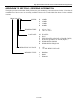
High-Speed Microcontroller User’s Guide: DS80C390 Supplement ADDENDUM TO SECTION 2: ORDERING INFORMATION The high-speed microcontroller family follows the part numbering convention shown below. Note that all combinations of devices are not currently available. Please refer to individual data sheets for the available versions.
High-Speed Microcontroller User’s Guide: DS80C390 Supplement ADDENDUM TO SECTION 4: PROGRAMMING MODEL The DS80C390 microprocessor is based on the industry standard 80C52. The core is an accumulatorbased architecture using internal registers for data storage and peripheral control. It executes the standard 8051 instruction set. This section provides a brief description of each architecture feature. Details concerning the programming model, instruction set, and register description are provided in Section 4.
High-Speed Microcontroller User’s Guide: DS80C390 Supplement register. Since there are four banks, the currently selected bank will be used by any instruction using R0R7. This allows software to change context by simply switching banks. The Working Registers also allow their contents to be used for indirect addressing of the upper 128 bytes of RAM. Thus an instruction can designate the value stored in R0 (for example) to address the upper RAM. This value might be the result of another calculation.
High-Speed Microcontroller User’s Guide: DS80C390 Supplement Figure 4-1.
High-Speed Microcontroller User’s Guide: DS80C390 Supplement SPECIAL FUNCTION REGISTERS Most of the unique features of the high-speed microcontroller family are controlled by bits in special function registers (SFRs) located in unused locations in the 8051 SFR map. This allows for increased functionality while maintaining complete instruction set compatibility. The SFRs reside in register locations 80h-FFh and are accessed using direct addressing. SFRs that end in 0 or 8 are bit addressable.
High-Speed Microcontroller User’s Guide: DS80C390 Supplement REGISTER BIT 7 SADDR0 SADDR1 C0M1C MSRDY C0M2C MSRDY C0M3C MSRDY C0M4C MSRDY C0M5C MSRDY P3 RD /P3.
High-Speed Microcontroller User’s Guide: DS80C390 Supplement REGISTER MXAX C1M1C C1M2C C1M3C C1M4C C1M5C B C1M6C C1M7C C1M8C C1M9C C1M10C EIP C1M11C C1M12C C1M13C C1M14C C1M15C BIT 7 BIT 6 BIT 5 BIT 4 BIT 3 BIT 2 BIT 1 BIT 0 ADDRESS MSRDY MSRDY MSRDY MSRDY MSRDY ETI ETI ETI ETI ETI ERI ERI ERI ERI ERI INTRQ INTRQ INTRQ INTRQ INTRQ EXTRQ EXTRQ EXTRQ EXTRQ EXTRQ MTRQ MTRQ MTRQ MTRQ MTRQ ROW/TIH ROW/TIH ROW/TIH ROW/TIH ROW/TIH DTUP DTUP DTUP DTUP DTUP MSRDY MSRDY MSRDY MSRDY MSRDY CANBIP MSR
High-Speed Microcontroller User’s Guide: DS80C390 Supplement REGISTER BIT 7 BIT 6 BIT 5 BIT 4 BIT 3 BIT 2 BIT 1 BIT 0 ADDRESS P5CNT C0C C0S C0IR C0TE C0RE IE SADDR0 SADDR1 C0M1C C0M2C C0M3C C0M4C C0M5C P3 C0M6C C0M7C C0M8C C0M9C C0M10C IP SADEN0 SADEN1 C0M11C C0M12C C0M13C C0M14C C0M15C SCON1 SBUF1 PMR STATUS MCON TA T2CON T2MOD RCAP2L RCAP2H TL2 TH2 COR PSW MCNT0 MCNT1 MA MB MC C1RMS0 C1RMS1 WDCON C1TMA0 C1TMA1 ACC 0 0 0 0 0 0 0 0 0 0 0 0 0 0 1 0 0 0 0 0 1 0 0 0 0 0 0 0 0 0 1 0 0 1 0 1 0 0 0 0 0
High-Speed Microcontroller User’s Guide: DS80C390 Supplement REGISTER BIT 7 BIT 6 BIT 5 BIT 4 BIT 3 BIT 2 BIT 1 BIT 0 ADDRESS C1C C1S C1IR C1TE C1RE EIE MXAX C1M1C C1M2C C1M3C C1M4C C1M5C B C1M6C C1M7C C1M8C C1M9C C1M10C EIP C1M11C C1M12C C1M13C C1M14C C1M15C 0 0 0 0 0 0 0 0 0 0 0 0 0 0 0 0 0 0 0 0 0 0 0 0 0 0 0 0 0 0 0 0 0 0 0 0 0 0 0 0 0 0 0 0 0 0 0 0 0 0 0 0 0 0 0 0 0 0 0 0 0 0 0 0 0 0 0 0 0 0 0 0 0 0 0 0 0 0 0 0 0 0 0 0 0 0 0 0 0 0 0 0 0 0 0 0 1 0 0 0 0 0 0 0 0 0 0 0 0 0 0 0 0 0 0 0 0 0 0
High-Speed Microcontroller User’s Guide: DS80C390 Supplement PORT 4 (P4) 7 SFR 80h 6 5 4 A19/P4.7 A18/P4.6 A17/P4.5 A18/P4.4 RW-0 RW-0 RW-0 RW-0 3 2 1 0 CE3 /P4.3 CE2 /P4.2 CE1 /P4.1 CE0 /P4.0 RW-1 RW-1 RW-1 RW-1 R = Unrestricted Read, W = Unrestricted Write, -n = Value after Reset P4.7–P4.0 A19 Bit 7 A18 Bit 6 A17 Bit 5 A16 Bit 4 CE3 Bit 3 Port 4. This port functions as a general-purpose I/O port.
High-Speed Microcontroller User’s Guide: DS80C390 Supplement STACK POINTER (SP) SFR 81h 7 6 5 4 3 2 1 0 SP.7 SP.6 SP.5 SP.4 SP.3 SP.2 SP.1 SP.0 RW-0 RW-0 RW-0 RW-0 RW-0 RW-1 RW-1 RW-1 R = Unrestricted Read, W = Unrestricted Write, -n = Value after Reset Stack Pointer. This stack pointer identifies current location of the stack. The stack pointer is incremented before every PUSH operation. This register defaults to 07h after reset.
High-Speed Microcontroller User’s Guide: DS80C390 Supplement DATA POINTER HIGH 1 (DPH1) SFR 85h 7 6 5 4 3 DPH1.7 DPH1.6 DPH1.5 DPH1.4 DPH1.3 RW-0 RW-0 RW-0 RW-0 RW-0 2 DPH1.2 RW-0 1 0 DPH1.1 DPH1.0 RW-0 RW-0 R = Unrestricted Read, W = Unrestricted Write, -n = Value after Reset Data Pointer High 1. This register is the high byte of the auxiliary 16-bit data pointer. When the SEL bit (DPS.0) is set, DPL1 and DPH1 are used in place of DPL and DPH during DPTR operations. DPH1.
High-Speed Microcontroller User’s Guide: DS80C390 Supplement POWER CONTROL (PCON) SFR 87h 7 6 5 4 3 2 1 0 SMOD_0 SMOD0 OFDF ODFE FG1 FG0 STOP IDLE RW-0 RW-0 RW-0* RW-0 RW-0 RW-0 RW-0 RW-0 R = Unrestricted Read, W = Unrestricted Write, -n = Value after Reset, * = See description SMOD_0 Bit 7 SMOD0 Bit 6 OFDF Bit 5 OFDE Bit 4 GF1 Bit 3 GF0 Bit 2 STOP Bit 1 IDLE Bit 0 Serial Port 0 Baud Rate Doubler Enable.
High-Speed Microcontroller User’s Guide: DS80C390 Supplement TIMER/COUNTER CONTROL (TCON) SFR 88h 7 6 5 4 3 2 1 0 TF1 TR1 TF0 TR0 IE1 IT1 IE0 IT0 RW-0 RW-0 RW-0 RW-0 RW-0 RW-0 RW-0 RW-0 R = Unrestricted Read, W = Unrestricted Write, -n = Value after Reset TF1 Bit 7 Timer 1 Overflow Flag. This bit indicates when Timer 1 overflows its maximum count as defined by the current mode.
High-Speed Microcontroller User’s Guide: DS80C390 Supplement TIMER MODE CONTROL (TMOD) SFR 89h 7 6 5 4 3 2 1 0 GATE C/ T M1 M0 GATE C/ T M1 M0 RW-0 RW-0 RW-0 RW-0 RW-0 RW-0 RW-0 RW-0 R = Unrestricted Read, W = Unrestricted Write, -n = Value after Reset GATE Bit 7 C/ T Bit 6 M1, M0 Bits 5-4 GATE Bit 3 C/ T Bit 2 M1, M0 Bits 1-0 Timer 1 Gate Control. This bit enable/disables the ability of Timer 1 to increment.
High-Speed Microcontroller User’s Guide: DS80C390 Supplement TIMER 0 LSB (TL0) SFR 8Ah 7 6 5 4 3 2 1 0 TL0.7 TL0.6 TL0.5 TL0.4 TL0.3 TL0.2 TL0.1 TL0.0 RW-0 RW-0 RW-0 RW-0 RW-0 RW-0 RW-0 RW-0 R = Unrestricted Read, W = Unrestricted Write, -n = Value after Reset Timer 0 LSB. This register contains the least significant byte of Timer 0. TL0.7-0 Bits 7-0 TIMER 1 LSB (TL1) SFR 8Bh 7 6 5 4 3 2 1 0 TL1.7 TL1.6 TL1.5 TL1.4 TL1.3 TL1.2 TL1.1 TL1.
High-Speed Microcontroller User’s Guide: DS80C390 Supplement CLOCK CONTROL (CKCON) SFR 8Eh 7 6 5 4 3 2 1 0 WD1 WD0 T2M T1M T0M MD2 MD1 MD0 RW-0 RW-0 RW-0 RW-0 RW-0 RW-0 RW-0 RW-1 R = Unrestricted Read, W = Unrestricted Write, -n = Value after Reset WD1, WD0 Bits 7-6 Watchdog Timer Mode Select 1-0. These bits select the watchdog timer timeout period, which determines the timing of the watchdog timer interrupt and the watchdog timer reset.
High-Speed Microcontroller User’s Guide: DS80C390 Supplement MD2, MD1, MD0 Bits 2-0 Stretch MOVX Select 2-0. These bits select the time by which external MOVX cycles are to be stretched. This allows slower memory or peripherals to be accessed without using ports or manual software intervention. The RD or WR strobe will be stretched by the specified interval, which will be transparent to the software except for the increased time to execute to MOVX instruction.
High-Speed Microcontroller User’s Guide: DS80C390 Supplement RXD1 Bit 2 Serial Port 1 Receive. This pin receives the serial port 1 data in serial port modes 1, 2, 3 and is a bidirectional data transfer pin in serial port mode 0. T2EX Bit 1 Timer 2 Capture/Reload Trigger. A 1 to 0 transition on this pin will cause the value in the T2 registers to be transferred into the capture registers if enabled by EXEN2 (T2CON.3).
High-Speed Microcontroller User’s Guide: DS80C390 Supplement RGSL Bit 1 Ring Oscillator Select. This bit selects the clock source following a resume from Stop mode. Using the ring oscillator to resume from Stop mode allows almost instantaneous startup. This bit is cleared to 0 after a power-on reset, and unchanged by all other forms of reset. The state of this bit will be undefined on devices that do not incorporate a ring oscillator.
High-Speed Microcontroller User’s Guide: DS80C390 Supplement 110 I/O A18 A17 A16 512 kbytes 111 A19 A18 A17 A16 1 Mbytes Port Pin P4.3-P4.0 Configuration Control Bits. P4CNT.2-0 determine whether specific P4 pins function as program chip enable signals or I/O. The memory ranges for each CEx signal are determined by P4CNT.5-3. Note that when the appropriate PDCEx bit (MCON.
High-Speed Microcontroller User’s Guide: DS80C390 Supplement CAN 0 RECEIVE MESSAGE STORED REGISTER 0 (C0RMS0) SFR 96h 7 C0RMS0.7 R-0 6 C0RMS0.6 R-0 5 C0RMS0.5 R-0 4 C0RMS0.4 R-0 3 C0RMS0.3 R-0 2 C0RMS0.2 R-0 1 C0RMS0.1 R-0 0 C0RMS0.0 R-0 R = Unrestricted Read, -n = Value after Reset CAN 0 Receive Message Stored Register 0. This register indicates which of CAN 0 message centers 1-8 have successfully received and stored a message since the last read of this register.
High-Speed Microcontroller User’s Guide: DS80C390 Supplement CAN 0 RECEIVE MESSAGE STORED REGISTER 1 (C0RMS1) 7 6 5 4 3 2 1 0 R-0 R-0 R-0 R-0 R-0 R-0 R-0 R-0 SFR 97h R = Unrestricted Read, -n = Value after Reset CAN 0 Receive Message Stored Register 1. This register indicates which of CAN 0 message centers 9-15 have successfully received and stored a message since the last read of this register.
High-Speed Microcontroller User’s Guide: DS80C390 Supplement SERIAL PORT 0 CONTROL (SCON0) SFR 98h 7 6 5 4 3 2 1 0 SM0/FE_0 SM1_0 SM2_0 REN_0 TB8_0 RB8_0 T1_0 R1_0 RW-0 RW-0 RW-0 RW-0 RW-0 RW-0 RW-0 RW-0 R = Unrestricted Read, W = Unrestricted Write, -n = Value after Reset Serial Port Mode. These bits control the mode of serial port 0. In addition the SM0 and SM2_0 bits have secondary functions as shown below.
High-Speed Microcontroller User’s Guide: DS80C390 Supplement TB8_0 Bit 3 9th Transmission Bit State. This bit defines the state of the 9th transmission bit in serial port 0 modes 2 and 3. RB8_0 Bit 2 9th Received Bit State. This bit identifies that state of the 9th reception bit of received data in serial port 0 modes 2 and 3. In serial port mode 1, when SM2_0=0, RB8_0 is the state of the stop bit. RB8_0 is not used in mode 0. TI_0 Bit 1 Transmitter Interrupt Flag.
High-Speed Microcontroller User’s Guide: DS80C390 Supplement EXTENDED STACK POINTER REGISTER (ESP) SFR 9Bh 7 6 5 4 3 2 1 0 1 1 1 1 1 1 ESP.1 ESP.0 R-1 R-1 R-1 R-1 R-1 R-1 RW-0 RW-0 R = Unrestricted Read, W = Unrestricted Write, -n = Value after Reset Reserved Extended Stack Pointer. This register contains the upper 2 bits of the 10-bit stack pointer.
High-Speed Microcontroller User’s Guide: DS80C390 Supplement ADDRESS CONTROL REGISTER (ACON) SFR 9Dh 7 6 5 4 3 2 1 0 1 1 1 1 1 SA AM1 AM0 R-1 R-1 R-1 R-1 R-1 RT-0 RT-0 RT-0 R = Unrestricted Read, T = Timed Access Write Only, -n = Value after Reset Bits 7-3 Reserved SA Bit 2 Extended Stack Address Mode Enable. This bit can only be modified by the timed-access procedure. 0 = All instructions will utilize the traditional 8-bit 8051 stack pointer (SP;81h).
High-Speed Microcontroller User’s Guide: DS80C390 Supplement CAN 0 TRANSMIT MESSAGE ACKNOWLEDGEMENT REGISTER 0 (C0TMA0) 7 6 5 4 3 2 1 0 R-0 R-0 R-0 R-0 R-0 R-0 R-0 R-0 SFR 9Eh R = Unrestricted Read, -n = Value after Reset CAN 0 Transmit Message Acknowledgement Register 0. This register indicates which of CAN 0 message centers 1-8 have successfully transmitted a message since the last read of this register.
High-Speed Microcontroller User’s Guide: DS80C390 Supplement CAN 0 TRANSMIT MESSAGE ACKNOWLEDGEMENT REGISTER 1 (C0TMA1) 7 6 5 4 3 2 1 0 R-0 R-0 R-0 R-0 R-0 R-0 R-0 R-0 SFR 9Fh R = Unrestricted Read, -n = Value after Reset CAN 0 Transmit Message Acknowledgement Register 1. This register indicates which of CAN 0 message centers 9-15 have successfully transmitted a message since the last read of this register.
High-Speed Microcontroller User’s Guide: DS80C390 Supplement PORT 2 (P2) 7 SFR A0h 6 5 4 3 2 A15/P2.7 A14/P2.6 A13/P2.5 A12/P2.4 A11/P2.3 A10/P2.2 RW-1 RW-1 RW-1 RW-1 RW-1 RW-1 1 0 A9/P2.1 A8/P2.0 RW-1 RW-1 R = Unrestricted Read, W = Unrestricted Write, -n = Value after Reset Port 2. The Port 2 pins function as an address bus during external memory accesses, and a general-purpose I/O port when executing code memory from the internal 4kB SRAM (IDM1,IDM0 = 00b).
High-Speed Microcontroller User’s Guide: DS80C390 Supplement External Connection bit (SP1EC, P5CNT.5) configures this pin as the Serial Port 1 receive signal, disabling the corresponding CAN 1 function. C0RX Bit 1 CAN 0 Receive. This pin is connected to the receive data output pin of the CAN 0 transceiver device. C0TX Bit 0 CAN 0 Transmit. This pin is connected to the transmit data input pin of the CAN 0 transceiver device.
High-Speed Microcontroller User’s Guide: DS80C390 Supplement established by the P4CNT register. Note that the chip-enable range when using A0-A15 is 32kB instead of the expected 64kB. This is to allow the use of more common 32kB memory devices rather than 64kB devices. Port 5 Pin Function P5CNT.2-0 P5.7 P5.6 P5.5 P5.
High-Speed Microcontroller User’s Guide: DS80C390 Supplement Reserved Bit 4 CRST Bit 3 AUTOB Bit 2 power-down mode. Power-down mode is exited by clearing the PDE bit or by any reset of the microcontroller. The CAN 0 module will resume operation after the receipt of 11 consecutive recessive bits. This bit is reserved and must always remain 0. Attempts to set the bit to 1 will cause improper device operation. CAN 0 Reset.
High-Speed Microcontroller User’s Guide: DS80C390 Supplement ERCS Bit 1 SWINT Bit 0 CAN 0 Error Count Select. This bit selects the number of transmit or receive errors that will cause the CAN 0 Error Count Exceeded bit, CECE (C0S.6), to be set. 0 = CECE bit set when the transmit or receive error counters exceed 9 errors. 1 = CECE bit set when the transmit or receive error counters exceed 127 errors. CAN 0 Software Initialization Enable.
High-Speed Microcontroller User’s Guide: DS80C390 Supplement CAN 0 STATUS REGISTER (C0S) SFR A4h 7 6 5 4 3 2 1 0 BUSOFF CECE WKS RXS TXS ER2 ER1 ER0 R-0 R-0 R-0 RW-0 RW-0 R-0 R-0 R-0 R = Unrestricted Read, W = Unrestricted Write, -n = Value after Reset BUSOFF Bit 7 CECE Bit 6 CAN 0 Bus Off. When BUSOFF = 1, the CAN 0 Bus is disabled and is not capable of receiving or transmitting messages. This condition is the result of the transmit error counter reaching a count of 256.
High-Speed Microcontroller User’s Guide: DS80C390 Supplement RXS Bit 4 CAN 0 Receive Status. This bit indicates whether or not messages have been received since the last read of the CAN 0 Status Register. RXS is only set by the CAN 0 logic and must be cleared by the Microcontroller software, the CRST bit, or a system Reset. 1 = The meaning of RXS=1 is dependent on the Autobaud bit, AUTOB.
High-Speed Microcontroller User’s Guide: DS80C390 Supplement ER2-0 Bit 2-0 TXS bit in the Status Register, a second status change interrupt flag will be set, issuing a second interrupt. Each new successful transmission generates an interrupt request independent of the previous state of the TXS bit, as long as the CAN Status Register has been read to clear the previous status change interrupt flag.
High-Speed Microcontroller User’s Guide: DS80C390 Supplement arbitration field (identifier and remote retransmission request). Bit 0 Error: Indicates that the CAN attempted to transmit a message and that when a dominant bit was transmitted, the CAN bus was found to have a recessive bit level. This error is not generated when the bit is a part of the arbitration field. The Bit 0 Error is set each time a recessive bit is received during the Busoff recovery period.
High-Speed Microcontroller User’s Guide: DS80C390 Supplement first interrupt source detected by the CAN module following the non-active interrupt state. The C0IR interrupt values will remain in place until the interrupt source is removed, independent of other higher (or lower) priority interrupts that become active prior to clearing the currently displayed interrupt source. When the current CAN interrupt source is cleared, C0IR will change to reflect the next active interrupt with the highest priority.
High-Speed Microcontroller User’s Guide: DS80C390 Supplement CAN 0 RECEIVE ERROR REGISTER (C0RE) 7 6 5 4 3 2 1 0 R*-0 R*-0 R*-0 R*-0 R*-0 R*-0 R*-0 R*-0 SFR A7h R= Unrestricted Read, * = Write only by C0TE register, -n = Value after Reset CAN 0 Receive Error Register. This register indicates the number of accumulated CAN 0 receive errors. All writes to the C0TE register are simultaneously loaded into this register.
High-Speed Microcontroller User’s Guide: DS80C390 Supplement Enable Timer 0 Interrupt. This bit controls the masking of the Timer 0 interrupt. 0 = Disable all Timer 0 interrupts. 1 = Enable all interrupt requests generated by the TF0 flag (TCON.5). Enable External Interrupt 0. This bit controls the masking of external interrupt 0. 0 = Disable external interrupt 0. 1 = Enable all interrupt requests generated by the INT0 pin.
High-Speed Microcontroller User’s Guide: DS80C390 Supplement CAN 0 MESSAGE CENTER 1 CONTROL REGISTER (C0M1C) SFR ABh 7 MSRDY RW-0 6 ETI RW-0 5 ERI RW-0 4 INTRQ RW-0 3 EXTRQ RC-0 2 MTRQ R*-0 1 ROW/TIH R*-0 0 DTUP R*-0 R = Unrestricted Read, C = Clear Only, * = See description below, -n = Value after Reset MSRDY Bit 7 ETI Bit 6 CAN 0 Message Center 1 Ready.
High-Speed Microcontroller User’s Guide: DS80C390 Supplement transmission by a message center programmed for transmission (T/ R = 1), the EXTRQ bit will be cleared by the CAN 0 controller. A remote request is only answered by a message center programmed for transmission (T/ R = 1) when DTUP = 1 and TIH = 0, i.e. when new data was loaded and is not being currently modified by the micro.
High-Speed Microcontroller User’s Guide: DS80C390 Supplement center when the CAN is processing the incoming data. ROW is cleared by the CAN module when software clears the DTUP bit associated with that message center. INTRQ is automatically set when the ERI=1 and message center 1 successfully receives and stores a message. ROW will reflect the actual message center relationships for message centers 1 to 14.
High-Speed Microcontroller User’s Guide: DS80C390 Supplement after the message center read. If DTUP has been set, then a new message was received and software should read the message center again to read the new data. If DTUP remained cleared, no additional data was received and the data is complete. If WTOE=0 the processor is not permitted to overwrite this message center, so it is only necessary to clear the DTUP bit after reading the message center.
High-Speed Microcontroller User’s Guide: DS80C390 Supplement CAN 0 MESSAGE CENTER 4 CONTROL REGISTER (C0M4C) SFR AEh 7 6 5 4 3 2 1 0 MSRDY ETI ERI INTRQ EXTRQ MTRQ ROW/TIH DTUP RW-0 RW-0 RW-0 RW-0 RC-0 R*-0 R*-0 R*-0 R = Unrestricted Read, C = Clear Only, * = See description below, -n = Value after Reset Operation of the bits in this register are identical to those found in the CAN 0 Message One Control Register (C0M1C;ABh).
High-Speed Microcontroller User’s Guide: DS80C390 Supplement INT0 Bit 2 TXD0 Bit 1 RXD0 Bit 0 External Interrupt 0. A falling edge/low level on this pin will cause an external interrupt 0 if enabled. Serial Port 0 Transmit. This pin transmits the serial port 0 data in serial port modes 1, 2, 3 and emits the synchronizing clock in serial port mode 0. Serial Port 0 Receive. This pin receives the serial port 0 data in serial port modes 1, 2, 3 and is a bidirectional data transfer pin in serial port mode 0.
High-Speed Microcontroller User’s Guide: DS80C390 Supplement CAN 0 MESSAGE CENTER 9 CONTROL REGISTER (C0M9C) SFR B6h 7 6 5 4 3 2 1 0 MSRDY ETI ERI INTRQ EXTRQ MTRQ ROW/TIH DTUP RW-0 RW-0 RW-0 RW-0 RC-0 R*-0 R*-0 R*-0 R = Unrestricted Read, C = Clear Only, * = See description below, -n = Value after Reset Operation of the bits in this register are identical to those found in the CAN 0 Message One Control Register (C0M1C;ABh).
High-Speed Microcontroller User’s Guide: DS80C390 Supplement Timer 0 Interrupt. This bit controls the priority of Timer 0 interrupt. 0 = Timer 0 is determined by the natural priority order. 1 = Timer 0 is a high priority interrupt. External Interrupt 0. This bit controls the priority of external interrupt 0. 0 = External interrupt 0 is determined by the natural priority order. 1 = External interrupt 0 is a high priority interrupt.
High-Speed Microcontroller User’s Guide: DS80C390 Supplement CAN 0 MESSAGE CENTER 11 CONTROL REGISTER (C0M11C) SFR BBh 7 6 5 4 3 2 1 0 MSRDY ETI ERI INTRQ EXTRQ MTRQ ROW/TIH DTUP RW-0 RW-0 RW-0 RW-0 RC-0 R*-0 R*-0 R*-0 R = Unrestricted Read, C = Clear Only, * = See description below, -n = Value after Reset Operation of the bits in this register are identical to those found in the CAN 0 Message One Control Register (C0M1C;ABh).
High-Speed Microcontroller User’s Guide: DS80C390 Supplement CAN 0 MESSAGE CENTER 15 CONTROL REGISTER (C0M15C) SFR BFh 7 6 5 4 3 2 1 0 MSRDY ETI ERI INTRQ EXTRQ MTRQ ROW/TIH DTUP RW-0 RW-0 RW-0 RW-0 RC-0 R*-0 R*-0 R*-0 R = Unrestricted Read, C = Clear Only, * = See description below, -n = Value after Reset Operation of the bits in this register are identical to those found in the CAN 0 Message One Control Register (C0M1C;ABh).
High-Speed Microcontroller User’s Guide: DS80C390 Supplement Mode 1: When set, reception is ignored (RI_1 is not set) if invalid stop bit received. Mode 2/3: When this bit is set, multiprocessor communications are enabled in modes 2 and 3. This will prevent the RI_1 bit from being set, and an interrupt being asserted, if the 9th bit received is not 1. Receive Enable. This bit enables/disables the serial port 1 receiver shift register. 0 = Serial port 1 reception disabled.
High-Speed Microcontroller User’s Guide: DS80C390 Supplement POWER MANAGEMENT REGISTER (PMR) SFR C4h 7 6 5 4 3 2 1 0 CD1 CD0 SWB CTM 4X/ 2X ALEOFF 1 1 R*-1 R*-0 RW-0 R*-0 R*-0 RW-0 R-1 R-1 R = Unrestricted Read, W = Unrestricted Write, * = See description below, -n = Value after Reset CD1, CD0 Bits 7-6 CD1:0 4X/ 2X 00 00 01 10 11 SWB Bit 5 CTM Bit 4 1 0 x x x Clock Divide Control 1-0.
High-Speed Microcontroller User’s Guide: DS80C390 Supplement 2. Set the CTM bit. At this point the CKRY bit (EXIF.3) will be cleared, indicating the internal clock stabilization period has commenced. Software is prohibited from modifying the CD1, CD0 bits while the CKRY bit is cleared. 3. Poll the CKRY bit until it is set. 4. Change CD0, CD1 bits to 00b. CTM cannot be changed from a 1 to a 0 while the Crystal Clock Multiplier option is selected by the CD1 and CD0 clock control bits.
High-Speed Microcontroller User’s Guide: DS80C390 Supplement Serial Port 0 Transmit Activity Monitor. When set, this bit indicates that data is currently being transmitted by serial port 0. It is cleared when the internal hardware sets the TI_1 bit. Do not alter the Clock Divide Control bits (PMR.7-6) while this bit is set or serial port data may be lost. Serial Port 0 Receive Activity Monitor. When set, this bit indicates that data is currently being received by serial port 0.
High-Speed Microcontroller User’s Guide: DS80C390 Supplement PDCE2 Bit 2 Program/Data Chip Enable 2. This bit selects whether the CE2 signal functions as the chip enable for external program memory only (PDCE=0), or as a merged chip enable for program and data memory (PDCE=1). When PDCE=1, the microprocessor will use the PSEN signal instead of the RD signal when reading from external MOVX memory. The Port 4 Control register (P4CNT) determines the memory range associated with CE2 .
High-Speed Microcontroller User’s Guide: DS80C390 Supplement TIMER 2 CONTROL (T2CON) SFR C8h 7 TF2 RW-0 6 EXF2 RW-0 5 RCLK RW-0 4 TCLK RW-0 3 EXEN2 RW-0 2 TR2 RW-0 1 C/ T2 RW-0 0 CP/ RL2 RW-0 R = Unrestricted Read, W = Unrestricted Write, -n = Value after Reset Timer 2 Overflow Flag. This flag will be set when Timer 2 overflows from FFFFh or the count equal to the capture register in down count mode. It must be cleared by software. TF2 will only be set if RCLK and TCLK are both cleared to 0.
High-Speed Microcontroller User’s Guide: DS80C390 Supplement TR2 Bit 2 Timer 2 Run Control. This bit enables/disables the operation of timer 2. Halting this timer will preserve the current count in TH2, TL2. 0 = Timer 2 is halted. 1 = Timer 2 is enabled. C/ T2 Bit 1 Counter/Timer Select. This bit determines whether timer 2 will function as a timer or counter. Independent of this bit, timer 2 runs at 2 clocks per tick when used in either baud rate generator or clock output mode.
High-Speed Microcontroller User’s Guide: DS80C390 Supplement Down Count Enable. This bit, in conjunction with the T2EX pin, controls the direction that timer 2 counts in 16-bit auto-reload mode. DCEN T2EX DIRECTION 1 1 Up 1 0 Down 0 X Up DCEN Bit 0 TIMER 2 CAPTURE LSB (RCAP2L) SFR CAh 7 6 5 4 3 2 1 0 RCAP2L.7 RCAP2L.6 RCAP2L.5 RCAP2L.4 RCAP2L.3 RCAP2L.2 RCAP2L.1 RCAP2L.
High-Speed Microcontroller User’s Guide: DS80C390 Supplement TIMER 2 MSB (TH2) SFR CDh 7 6 5 4 3 2 1 0 TH2.7 TH2.6 TH2.5 TH2.4 TH2.3 TH2.2 TH2.1 TH2.0 RW-0 RW-0 RW-0 RW-0 RW-0 RW-0 RW-0 RW-0 R = Unrestricted Read, W = Unrestricted Write, -n = Value after Reset TL2.7-0 Bits 7-0 Timer 2 MSB. This register contains the least significant byte of Timer 2.
High-Speed Microcontroller User’s Guide: DS80C390 Supplement External Clock Output Enable. This bit enables the optional clock output functions on port pin P3.5. Associated bits are shown in the following table. CLKOE IRDACK COD1 COD0 P3.
High-Speed Microcontroller User’s Guide: DS80C390 Supplement MULTIPLIER CONTROL REGISTER ZERO (MCNT0) SFR D1h 7 LSHIFT RW-0 6 CSE RW-0 5 SCE RW-0 4 MAS4 RW-0 3 MAS3 RW-0 2 MAS2 RW-0 1 MAS1 RW-0 0 MAS0 RW-0 R = Unrestricted Read, W = Unrestricted Read, -n = Value after Reset LSHIFT Bit 7 CSE Bit 6 SCE Bit 5 Left Shift. This bit works in conjunction with the SCE and CSE bits to determine the direction and path of arithmetic accelerator shift operations as shown below.
High-Speed Microcontroller User’s Guide: DS80C390 Supplement Multiplier Register Shift Bits. These bits determine the number of shifts performed when a shift operation is performed with the arithmetic accelerator, and are also used to indicate how many shifts were performed during a previous normalization operation. These bits are cleared to 00000b following a system reset or the initialization of the arithmetic accelerator.
High-Speed Microcontroller User’s Guide: DS80C390 Supplement Clear Accelerator Registers. Writing a one to this bit will clear the MA, MB, and MC registers. Reading this bit will always return a logic 0. Reserved CLM Bit 4 Bit 3-0 MULTIPLIER A REGISTER (MA) 7 6 5 4 3 2 1 0 RW-0 RW-0 RW-0 RW-0 RW-0 RW-0 RW-0 RW-0 SFR D3h R = Unrestricted Read, W = Unrestricted Read, -n = Value after Reset Bits 7-0 Multiplier A Register.
High-Speed Microcontroller User’s Guide: DS80C390 Supplement MULTIPLIER C REGISTER (C) 7 6 5 4 3 2 1 0 RW-0 RW-0 RW-0 RW-0 RW-0 RW-0 RW-0 RW-0 SFR D5h R = Unrestricted Read, W = Unrestricted Read, -n = Value after Reset Bits 7-0 Multiplier C Register. The MC Register allows access to the 40-bit accumulator register for the arithmetic accelerator.
High-Speed Microcontroller User’s Guide: DS80C390 Supplement C1RMS0.2 Bit 2 C1RMS0.1 Bit 1 C1RMS0.0 Bit 0 Message Center 3, Message Received and Stored Message Center 2, Message Received and Stored Message Center 1, Message Received and Stored CAN 1 RECEIVE MESSAGE STORED REGISTER 1 (C1RMS1) 7 6 5 4 3 2 1 0 R-0 R-0 R-0 R-0 R-0 R-0 R-0 R-0 SFR D7h R = Unrestricted Read, -n = Value after Reset Bit 7 C1RMS1.6 Bit 6 C1RMS1.5 Bit 5 C1RMS1.4 Bit 4 C1RMS1.3 Bit 3 C1RMS1.2 Bit 2 C1RMS1.
High-Speed Microcontroller User’s Guide: DS80C390 Supplement WATCHDOG CONTROL (WDCON) SFR D8h 7 6 5 4 3 2 1 0 SMOD POR EPF1 PFI WDIF WTRF EWT RWT RW-0 RT-* RW-0 RW-* RT-0 RW-* RT-* RT-0 R = Unrestricted Read, W = Unrestricted Write, T = Timed Access Write Only, -n = Value after Reset, * = See Description SMOD Bit 7 POR Bit 6 EPFI Bit 5 PFI Bit 4 WDIF Bit 3 Serial Modification. This bit controls the doubling of the serial port 1 baud rate in modes 1, 2, and 3.
High-Speed Microcontroller User’s Guide: DS80C390 Supplement WTRF Bit 2 Watchdog Timer Reset Flag. When set, this bit indicates that a watchdog timer reset has occurred. It is typically interrogated to determine if a reset was caused by watchdog timer reset. It is cleared by a power- on reset, but otherwise must be cleared by software before the next reset of any kind or software may erroneously determine that a watchdog timer reset has occurred.
High-Speed Microcontroller User’s Guide: DS80C390 Supplement C1TMA0.3 Bit 3 C1TMA0.2 Bit 2 C1TMA0.1 Bit 1 C1TMA0.0 Bit 0 Message Center 4, Message Transmitted Message Center 3, Message Transmitted Message Center 2, Message Transmitted Message Center 1, Message Transmitted CAN 1 TRANSMIT MESSAGE ACKNOWLEDGEMENT REGISTER 1 (C1TMA1) SFR DFh 7 6 5 4 3 2 1 0 — — — — — — — — R-0 R-0 R-0 R-0 R-0 R-0 R-0 R-0 R = Unrestricted Read, -n = Value after Reset Bit 7 C1TMA1.6 Bit 6 C1TMA1.
High-Speed Microcontroller User’s Guide: DS80C390 Supplement ACCUMULATOR (A or ACC) SFR E0h 7 6 5 4 3 2 1 0 ACC.7 ACC.6 ACC.5 ACC.4 ACC.3 ACC.2 ACC.1 ACC.0 RW-0 RW-0 RW-0 RW-0 RW-0 RW-0 RW-0 RW-0 R = Unrestricted Read, W = Unrestricted Write, -n = Value after Reset Accumulator. This register serves as the accumulator for arithmetic operations. It is functionally identical to the accumulator found in the 80C32. ACC.
High-Speed Microcontroller User’s Guide: DS80C390 Supplement CRST Bit 3 AUTOB Bit 2 CAN 1 Reset. Setting this bit by a Timed Access write will reset all CAN 1 registers in the SFR map to their reset default states. The module will reset the registers immediately upon setting this bit, or following the completion of the current reception, transmission, arbitration failure, or error condition on CAN 1.
High-Speed Microcontroller User’s Guide: DS80C390 Supplement MOVX SRAM. These bytes contain the CAN 1 Control/Status/Mask Registers. Read access to all bytes in the CAN 1 MOVX SRAM is permitted at all times, regardless of the state of the SWINT bit. Setting SWINT=1 disables CAN 1 Bus activity, allowing software access to the CAN 1 Control/Status/Mask Registers without corrupting CAN Bus transmission or reception.
High-Speed Microcontroller User’s Guide: DS80C390 Supplement CAN 1 STATUS REGISTER (C1S) SFR E4h 7 BUSOFF R-0 6 CECE R-0 5 WKS R-0 4 RXS RW-0 3 TXS RW-0 2 ER2 R-0 1 ER1 R-0 0 ER0 R-0 R = Unrestricted Read, W = Unrestricted Write, -n = Value after Reset BUSOFF Bit 7 CECE Bit 6 CAN 1 Bus Off. When BUSOFF = 1, the CAN 1 Bus is disabled and is not capable of receiving or transmitting messages. This condition is the result of the transmit error counter reaching a count of 256.
High-Speed Microcontroller User’s Guide: DS80C390 Supplement or a system Reset. 1 = The meaning of RXS=1 is dependent on the autobaud bit, AUTOB. AUTOB=0, RXS = 1 indicates that a message has been both successfully received and stored in one of the message centers by CAN 1 since the last read of the CAN 1 Status Register. AUTOB=1, RXS = 1 indicates that a message has been successfully received by CAN 1 since the last read of the CAN 1 Status Register.
High-Speed Microcontroller User’s Guide: DS80C390 Supplement ER2-0 Bit 2-0 CAN Status Register has been read to clear the previous status change interrupt flag. Note that if software changes TXS from 0 to 1, an artificial Status Change Interrupt (STIE=1) will be generated. Thus, if TXS was previously set to 0 and a reception was successful, TXS will be set to 1 and an enabled interrupt may be asserted. An interrupt may be asserted (if enabled) if software changes TXS from 0 to 1.
High-Speed Microcontroller User’s Guide: DS80C390 Supplement CAN 1 INTERRUPT REGISTER (C1IR) 7 6 5 4 3 2 1 0 R-0 R-0 R-0 R-0 R-0 R-0 R-0 R-0 SFR E5h R = Unrestricted Read, W = Unrestricted Write, -n = Value after Reset C1IR.7-0 Bit 7-5 CAN 1 Interrupt Indicator 7-0 This register indicates the status of the interrupt source associated with the CAN 1 module. Reading this register after the generation of a CAN 1 Interrupt will identify the interrupt source as shown in the table below.
High-Speed Microcontroller User’s Guide: DS80C390 Supplement CAN 1 TRANSMIT ERROR REGISTER (C1TE) SFR E6h 7 6 5 4 3 2 1 0 — — — — — — — — R*-0 R*-0 R*-0 R*-0 R*-0 R*-0 R*-0 R*-0 R = Unrestricted Read, * = Write only when SWINT = 1 and BUSOFF = 0, -n = Value after Reset CAN 1 Transmit Error Register. This register indicates the number of accumulated CAN 1 transmit errors. The CAN 1 module responds in different ways to varying number of errors as shown below. C1TE.
High-Speed Microcontroller User’s Guide: DS80C390 Supplement EXTENDED INTERRUPT ENABLE (EIE) SFR E8h 7 6 5 4 3 2 1 0 CANBIE C0IE C1IE EWDI EX5 EX4 EX3 EX2 RW-0 RW-0 RW-0 RW-0 RW-0 RW-0 RW-0 RW-0 R = Unrestricted Read, W = Unrestricted Write, -n = Value after Reset CAN 0/1 Activity Interrupt Priority. This bit enables/disables the CAN 0/1 Activity Interrupt 0 = Disable the CAN 0/1 Activity Interrupt. 1 = Enable the CAN 0/1 Activity Interrupt. CAN 0 Interrupt Enable.
High-Speed Microcontroller User’s Guide: DS80C390 Supplement CAN 1 MESSAGE CENTER 1 CONTROL REGISTER (C1M1C) SFR EBh 7 MSRDY RW-0 6 ETI RW-0 5 ERI RW-0 4 INTRQ RW-0 3 EXTRQ RC-0 2 MTRQ R*-0 1 ROW/TIH R*-0 0 DTUP R*-0 R = Unrestricted Read, C = Clear Only, * = See description below, -n = Value after Reset MSRDY Bit 7 ETI Bit 6 ERI Bit 5 INTRQ Bit 4 EXTRQ Bit 3 CAN 1 Message Center 1 Ready.
High-Speed Microcontroller User’s Guide: DS80C390 Supplement MTRQ Bit 2 ROW/TIH Bit 1 EXTRQ bit in a similar manner, but will not automatically transmit a data frame and as such will not automatically clear the EXTRQ bit. CAN 1 Message Center 1 Microcontroller Transmit Request. When set, this bit indicates that the message center is requesting that a message be transmitted.
High-Speed Microcontroller User’s Guide: DS80C390 Supplement DTUP Bit 0 center, EXTRQ will be set to a 1. Following the Remote Frame Request and after the microcontroller has established the proper data to be sent, the microcontroller will clear the TIH bit to a 0, which will allow the CAN module to send the data requested by the previous Remote Frame Request. Note that the TIH bit associated with Message Center 15 is ignored because it is a receive-only message center.
High-Speed Microcontroller User’s Guide: DS80C390 Supplement CAN 1 MESSAGE CENTER 2 CONTROL REGISTER (C1M2C) SFR ECh 7 6 5 4 3 2 1 0 MSRDY ETI ERI INTRQ EXTRQ MTRQ ROW/TIH DTUP RW-0 RW-0 RW-0 RW-0 RC-0 R*-0 R*-0 R*-0 R = Unrestricted Read, C = Clear Only, * = See description below, -n = Value after Reset Operation of the bits in this register are identical to those found in the CAN 1 Message One Control Register (C1M1C;ABh).
High-Speed Microcontroller User’s Guide: DS80C390 Supplement B REGISTER (B) SFR F0h 7 6 5 4 3 2 1 0 B.7 B.6 B.5 B.4 B.3 B.2 B.1 B.0 RW-0 RW-0 RW-0 RW-0 RW-0 RW-0 RW-0 RW-0 R = Unrestricted Read, W = Unrestricted Write, -n = Value after Reset B Register. This register serves as a second accumulator for certain arithmetic operations. It is functionally identical to the B register found in the 80C32. B.
High-Speed Microcontroller User’s Guide: DS80C390 Supplement CAN 1 MESSAGE CENTER 9 CONTROL REGISTER (C1M9C) SFR F6h 7 6 5 4 3 2 1 0 MSRDY ETI ERI INTRQ EXTRQ MTRQ ROW/TIH DTUP RW-0 RW-0 RW-0 RW-0 RC-0 R*-0 R*-0 R*-0 R = Unrestricted Read, C = Clear Only, * = See description below, -n = Value after Reset Operation of the bits in this register are identical to those found in the CAN 1 Message One Control Register (C1M1C;ABh).
High-Speed Microcontroller User’s Guide: DS80C390 Supplement 1 = External interrupt 5 is a high priority interrupt. External Interrupt 4 Priority. This bit controls the priority of external interrupt 4. 0 = External interrupt 4 is a low priority interrupt. 1 = External interrupt 4 is a high priority interrupt. External Interrupt 3 Priority. This bit controls the priority of external interrupt 3. 0 = External interrupt 3 is a low priority interrupt. 1 = External interrupt 3 is a high priority interrupt.
High-Speed Microcontroller User’s Guide: DS80C390 Supplement CAN 1 MESSAGE CENTER 14 CONTROL REGISTER (C1M14C) SFR FEh 7 6 5 4 3 2 1 0 MSRDY ETI ERI INTRQ EXTRQ MTRQ ROW/TIH DTUP RW-0 RW-0 RW-0 RW-0 RC-0 R*-0 R*-0 R*-0 R = Unrestricted Read, C = Clear Only, * = See description below, -n = Value after Reset Operation of the bits in this register are identical to those found in the CAN 1 Message One Control Register (C1M1C;ABh).
High-Speed Microcontroller User’s Guide: DS80C390 Supplement ADDENDUM TO SECTION 5: CPU TIMING SYSTEM CLOCK SELECTION The internal clocking options of the DS80C390 differs slightly from that described in the High-Speed Microcontroller User’s Guide. Most members of the family offer the option of 4, 256, or 1024 oscillator clocks per machine cycle. The DS80C390 can operate at 1, 2, 4, or 1024 clocks per machine cycle. The logical operation of the system clock divide control function is shown below.
High-Speed Microcontroller User’s Guide: DS80C390 Supplement Table 5-1. SYSTEM CLOCK CONFIGURATION CD1 CD0 4X/ 2X 0 0 0 1 1 0 0 1 0 1 0 1 N/A N/A N/A NAME CLOCKS/MC Frequency Multiplier (2X) Frequency Multiplier (4X) Reserved Divide-by-4 (Default) Power Management Mode 2 1 — 4 1024 MAX EXTERNAL FREQUENCY (MHz) 20 10 — 40 40 The system clock and machine cycle rate changes one machine cycle after the instruction changing the control bits.
High-Speed Microcontroller User’s Guide: DS80C390 Supplement ADDENDUM TO SECTION 6: MEMORY ACCESS EXTERNAL MEMORY INTERFACING The DS80C390 follows the memory interface convention established by the industry standard 80C32/80C52, but with many added improvements. Most notably, the device incorporates a 22-bit addressing capability that supports up to four megabytes of program memory and four megabytes of data memory.
High-Speed Microcontroller User’s Guide: DS80C390 Supplement Table 6-2. EXTENDED ADDRESS AND CHIP ENABLE GENERATION Port 4 Pin Function Port 4 Pin Function (A19-A16 Address Pins) (Code Memory Chip Enables) P4CNT.5-3 P4.7 P4.6 P4.5 P4.4 P4CNT.2-0 P4.3 P4.2 P4.1 P4.0 000 I/O I/O I/O I/O 000 I/O I/O I/O I/O 100 I/O I/O I/O A16 100 I/O I/O I/O CE0 101 I/O I/O A17 A16 101 I/O I/O CE1 CE0 110 I/O A18 A17 A16 110 I/O CE2 CE1 CE0 111(default) A19 A18 A17 A16 111(default) CE3 CE2 CE1 CE0 P5CNT.
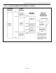
High-Speed Microcontroller User’s Guide: DS80C390 Supplement IMPLEMENTING A BOOTLOADER USING INTERNAL SRAM The internal 4 KB SRAM of the DS80C390 can be used to implement a bootloader function, allowing insystem reprogrammability. One of the difficulties of implementing a bootloader function with a Flash memory device is that the Flash programming algorithm will not allow instruction fetches (reads) from a device while it is being reprogrammed.
High-Speed Microcontroller User’s Guide: DS80C390 Supplement Figure 6-1. EXAMPLE DS80C390 PROGRAM/DATA MEMORY INTERFACE P1.6/A6 P1.5/A5 P1.4/A4 P1.3/A3 P1.2/A2 P1.1/A1 P1.0/A0 GND VCC AD0/D0 AD1/D1 AD2/D2 AD3/D3 AD4/D4 AD5/D5 AD6/D6 512k X 8 FLASH PROGRAM MEMORY DS80C390 AD7/D7 EA\ ALE PSEN\ P2.7\A15 P2.6\A14 P2.5\A13 GND VCC P2.4/A12 P2.3/A11 P2.2/A10 P2.1/A9 P2.0/A8 P4.0/CE0\ P4.1/CE1\ P5.4/PCE0\ P5.3/C1TX P5.2/C1RX P5.1/C0RX P5.0/C0TX VCC XTAL2 XTAL1 GND MUX\ P4.7/A19 P4.6/A18 P4.5/A17 P4.4/A16 P4.
High-Speed Microcontroller User’s Guide: DS80C390 Supplement Figure 6-2.
High-Speed Microcontroller User’s Guide: DS80C390 Supplement Figure 6-3.
High-Speed Microcontroller User’s Guide: DS80C390 Supplement Having selected the memory configuration, the following SFR settings affect the example memory map: SA IDM CMA EQU 1 EQU 2 EQU 1 P4CNT5_3 P4CNT2_0 P5CNT2_0 EQU 110B EQU 101B EQU 110B ; ; ; ; ; ; ; Use 1KB stack in on-chip XDATA space 2 = 4KB on-chip SRAM location X:0x400000 – X:400FFF 1 = CAN0 X:0x401000 – X:0x4010FF CAN1 X:0x401100 – X:0x4011FF 110B = 512kB (A18-A0 enabled) 101B = enable CE0, CE1 110B = enable PCE0, PCE1, PCE2 When complet
High-Speed Microcontroller User’s Guide: DS80C390 Supplement ADDENDUM TO SECTION 7: POWER MANAGEMENT The DS80C390 supports the general power management features of the DS87C520 described in the HighSpeed Microcontroller User’s Guide. Exceptions are noted below. POWER MANAGEMENT MODES Power management mode 1 (PMM1) is not supported on the DS80C390. SWITCHING BETWEEN CLOCK SOURCES The ring oscillator on the DS80C390 is similar to that on the DS80C320.
High-Speed Microcontroller User’s Guide: DS80C390 Supplement ADDENDUM TO SECTION 8: RESET CONDITIONS This section supersedes the corresponding section in the High-Speed Microcontroller User’s Guide. The microprocessor provides several ways to place the CPU in a reset state. It also offers the means for software to determine the cause of a reset. The reset state of most processor bits is not dependent on the type of reset, but selected bits do depend on the reset source.
High-Speed Microcontroller User’s Guide: DS80C390 Supplement EXTERNAL RESET If the RST input is taken to a logic 1, the CPU will be forced into a reset state. This will not occur instantaneously, as the condition must be detected and then clocked into the microprocessor. It requires a minimum of two machine cycles to detect and invoke the reset state. Thus the reset is a synchronous operation and the crystal must be running to cause an external reset.
High-Speed Microcontroller User’s Guide: DS80C390 Supplement contents are not altered. Interrupts and Timers are disabled. The state of the Watchdog Timer is dependent on the specific device in use. Note that the Watchdog time out defaults to its shortest interval on any reset. I/O Ports are taken to a weak high state (FFh). This leaves each port pin configured with the data latch set to a 1.
High-Speed Microcontroller User’s Guide: DS80C390 Supplement ADDENDUM TO SECTION 10: PARALLEL I/O Changes to this section primarily involve the additional functionality associated with Port 4 and 5, and the use of Port 1 as the address LSB in nonmultiplexed memory mode. Because the DS80C390 is a ROMless device, Port 0 and 2 do not support general-purpose I/O.
High-Speed Microcontroller User’s Guide: DS80C390 Supplement OUTPUT FUNCTIONS Although 8051 I/O ports appear to be true I/O, their output characteristics are dependent on the individual port and pin conditions. When software writes a logic 0 to the port for output, the port is pulled to ground. When software writes a logic 1 to the port for output, ports 1, 3, 4, or 5 will drive weak pullups (after the strong transition from 0 to 1). Port 0 will go tri-state.
High-Speed Microcontroller User’s Guide: DS80C390 Supplement ADDENDUM TO SECTION 11: PROGRAMMABLE TIMERS The timers of the DS80C390 are very similar to the those of described in the High-Speed Microcontroller User’s Guide. The primary changes concern the removal of the PMM2 option and the inclusion of the frequency multiplier settings. The following figures replace the corresponding figures in Section 11 of the High-Speed Microcontroller User’s Guide.
High-Speed Microcontroller User’s Guide: DS80C390 Supplement TIMER/COUNTER 0 AND 1 MODE 2 T0M = CKCON.3 (T1M = CKCON.4) CD1:0 11 anything else OSC CLK OUT /3,072 /12 0 1 4X/ 2X CD1:0 CLK OUT 1 0 x x 00 00 10 11 C/T = TMOD.2 (C/T = TMOD.6) 0 /1 /2 /4 /1024 /CLK TL0 (TL1) 0 7 1 T0 = P3.4 (T1 = P3.5) TR0 = TCON.4 (TR1 = TCON.6) 0 TH0 (TH1) GATE = TMOD.3 (GATE = TMOD.7) 7 /INT0 = P3.2 (/INT1 = P3.3) TF0 = TCON.5 (TF1 = TCON.
High-Speed Microcontroller User’s Guide: DS80C390 Supplement TIMER/COUNTER 2 CLOCK-OUT MODE (/RL2 = 0) TIMER/COUNTER 2 BAUD RATE GENERATOR MODE /RL2(T2CON.0) = 0; RCLK (T2CON.5) = 1, or TCLK(T2CON.
High-Speed Microcontroller User’s Guide: DS80C390 Supplement TIMER/COUNTER 2 AUTO RELOAD MODE (/RL2 = 0) (A) DCEN = 0 TIMER/COUNTER 2 AUTO RELOAD MODE (/RL2 = 0) (B) DCEN = 1 109 of 158
High-Speed Microcontroller User’s Guide: DS80C390 Supplement DIVIDE-BY-13 OPTION The other change to the timers associated with the DS80C390 is the inclusion of a divide-by-13 option for Timer 1 and Timer 2. The option in independently enabled for each timer by setting the D13T1 (for timer 1) or D13T2 (for timer 2) bits. When enabled by setting the appropriate bits, the timer input from the T1 or T2 external pins will be replaced by a timebase that is OSC/13.
High-Speed Microcontroller User’s Guide: DS80C390 Supplement IrDA CLOCK OUTPUT The Infrared Data Association (IrDA) communication protocol is a popular way to connect physically separated devices up to one meter distant. The physical layer of the protocol is very easy to implement: configure the DS80C390’s serial port 0 by selecting crystal speed, baud rate, etc.
High-Speed Microcontroller User’s Guide: DS80C390 Supplement ADDENDUM TO SECTION 12: SERIAL I/O The serial ports of the DS80C390’s Ax and Bx versions operate the same as those described in the HighSpeed Microcontroller User’s Guide. Revision C3 and later devices will change the operation of serial port 1 as follows.
High-Speed Microcontroller User’s Guide: DS80C390 Supplement ADDENDUM TO SECTION 13: TIMED ACCESS PROTECTION A number of timed-access protected bits are associated with the new features of the DS80C390. Please consult the High-Speed Microcontroller User’s Guide for complete information on the use of the timedaccess feature. POR (WDCON.6): WDIF (WDCON.3): EWT (WDCON.1): RWT (WDCON.0): BGS (EXIF.0): SA (ACON.2): AM1-AM0 (ACON.1-ACON.0): IDM1-IDM0 (MCON.7-MCON.6): CMA (MCON.5): PDCE3-PDCE.0 (MCON.3-MCON.
High-Speed Microcontroller User’s Guide: DS80C390 Supplement ADDENDUM TO SECTION 16: INSTRUCTION SET DETAILS The DS80C390 supports one of three different address modes, selected by the AM1 and AM0 bits in the ACON register. The processor operates in either the traditional 16-bit address mode, 22-bit paged address mode or in a 22-bit contiguous address mode. When operating in the 16-bit addressing mode (AM1, AM0 = 00b), all instruction cycle timing and byte counts will be identical to the 8051 family.
High-Speed Microcontroller User’s Guide: DS80C390 Supplement The DS80C390 supports interrupts from any location in the 22-bit address field. When an interrupt request is acknowledged, the current contents of the 22-bit Program Counter (PC) is pushed onto the stack, and the page value (00h) and the lower 16-bit address of the interrupt vector is then written to the PC before the execution of the LCALL.
High-Speed Microcontroller User’s Guide: DS80C390 Supplement The modification of the instructions in the 22-bit page address mode is summarized in the following table.
High-Speed Microcontroller User’s Guide: DS80C390 Supplement software tools (assembler or compiler) specifically designed to accept the modified length of the new instructions. In addition, the 22-bit contiguous mode utilizes the MXAX register to supply the upper 8-bits of the 22bit (or 23-bit if CMA=1 or IDM1=) address bits of the MOVX address during register indirect MOVX instructions such as MOVX @Ri, A or MOVX A, @Ri. The complete address is formed by concatenating MXAX, P2, and R1 or R0 in this mode.
High-Speed Microcontroller User’s Guide: DS80C390 Supplement MNEMONIC D7 ACALL addr a18 19 a15 a7 INSTRUCTION CODE D6 D5 D4 D3 D2 D1 D0 a17 a16 1 0 0 0 1 a14 a13 a12 a11 a10 a9 a8 a6 a5 a4 a3 a2 a1 a0 AJMP addr 19 a18 a17 a16 0 0 0 0 a15 a14 a13 a12 a11 a10 a9 a7 a6 a5 a4 a3 a2 a1 INC DPTR 1 0 1 0 0 0 1 HEX Byte 1 Byte 2 Byte 3 1 a8 a0 1 Byte 1 Byte 2 Byte 3 A3 0 LCALL addr24 0 0 0 1 0 0 1 a23 a22 a21 a20 a19 a18 a17 a16 a15 a14 a13 a12 a11 a10 a9 a8 a7 a6 a5 a4 a3 a2 a1 a0 LJMP addr24 0 a23 a15 a7
High-Speed Microcontroller User’s Guide: DS80C390 Supplement SECTION 19: CONTROLLER AREA NETWORK (CAN) MODULE (DS80C390 Supplement Only) The DS80C390 incorporates two identical CAN controllers (CAN 0 and CAN 1). Each of these CAN units provides operating modes that are fully compliant with the CAN 2.0B specification. The microcontroller interface to the CAN controllers is broken into two groups of registers.
High-Speed Microcontroller User’s Guide: DS80C390 Supplement MOVX MESSAGE CENTERS FOR CAN 0 CAN 0 CONTROL/STATUS/MASK REGISTERS Register 7 6 5 4 3 2 1 0 MOVX Data Address1 C0MID0 MID07 MID06 MID05 MID04 MID03 MID02 MID01 MID00 xxxx00h C0MA0 M0AA7 M0AA6 M0AA5 M0AA4 M0AA3 M0AA2 M0AA1 M0AA0 xxxx01h C0MID1 MID17 MID10 xxxx02h C0MA1 M1AA7 M1AA6 M1AA5 M1AA4 M1AA3 M1AA2 M1AA1 M1AA0 xxxx03h MID16 SJW0 MID15 BPR5 MID14 BPR4 MID13 BPR3 MID12 BPR2 MID11 C0BT0 SJW1 BPR1 BPR0 C0B
High-Speed Microcontroller User’s Guide: DS80C390 Supplement CAN 0 MESSAGE CENTERS 2-14 MESSAGE CENTER 2 REGISTERS (similar to Message Center 1) xxxx20h - 2Fh MESSAGE CENTER 3 REGISTERS (similar to Message Center 1) xxxx30h - 3Fh MESSAGE CENTER 4 REGISTERS (similar to Message Center 1) xxxx40h - 4Fh MESSAGE CENTER 5 REGISTERS (similar to Message Center 1) xxxx50h - 5Fh MESSAGE CENTER 6 REGISTERS (similar to Message Center 1) xxxx60h - 6Fh MESSAGE CENTER 7 REGISTERS (similar to Message Center 1)
High-Speed Microcontroller User’s Guide: DS80C390 Supplement MOVX MESSAGE CENTERS FOR CAN 1 CAN 1 CONTROL/STATUS/MASK REGISTERS Register 7 6 5 4 3 2 1 0 MOVX Data Address1 C1MID0 MID07 MID06 MID05 MID04 MID03 MID02 MID01 MID00 xxxx00h C1MA0 M0AA7 M0AA6 M0AA5 M0AA4 M0AA3 M0AA2 M0AA1 M0AA0 xxxx01h C1MID1 MID17 MID16 MID15 MID14 MID13 MID12 MID11 MID10 xxxx02h C1MA1 M1AA7 M1AA6 M1AA5 M1AA4 M1AA3 M1AA2 M1AA1 M1AA0 xxxx03h C1BT0 SJW1 SJW0 BPR5 BPR4 BPR3 BPR2 BPR1 BPR0 C1BT1 SMP
High-Speed Microcontroller User’s Guide: DS80C390 Supplement CAN 1 MESSAGE CENTERS 2-14 MESSAGE CENTER 2 REGISTERS (similar to Message Center 1) xxxx20h - 2Fh MESSAGE CENTER 3 REGISTERS (similar to Message Center 1) xxxx30h - 3Fh MESSAGE CENTER 4 REGISTERS (similar to Message Center 1) xxxx40h - 4Fh MESSAGE CENTER 5 REGISTERS (similar to Message Center 1) xxxx50h - 5Fh MESSAGE CENTER 6 REGISTERS (similar to Message Center 1) xxxx60h - 6Fh MESSAGE CENTER 7 REGISTERS (similar to Message Center 1)
High-Speed Microcontroller User’s Guide: DS80C390 Supplement CAN MOVX REGISTER DESCRIPTION Most of the SRAM control registers, including the message centers proper, are mapped into a special location in the MOVX SRAM space. The specific location of the registers is a function of the module number (CAN 0 or CAN 1) and the CMA bit that controls whether the CAN SRAM begins at location 401xxxh or 00Exxxh. The MOVX CAN Registers consist of a set of one Control/Status/Mask register and 15 message centers.
High-Speed Microcontroller User’s Guide: DS80C390 Supplement CnMID0 masks programmed to 1 will force the state of the corresponding Data Byte bit and CAN Media Byte Arbitration Registers 1 and 0 to match before considering the incoming message a match. Programming either Media ID Mask Register to 00h effectively disables the Media ID test for that byte. As such the CnMID1, CnMID0 masks act as a don’t care following a system Reset.
High-Speed Microcontroller User’s Guide: DS80C390 Supplement can only be modified during a software initialization (SWINT=1). BPR5 BPR4 BPR3 BPR2 BPR1 BPR0 0 0 . . 1 1 0 0 . . 1 1 0 0 . . 1 1 0 0 . . 1 1 0 0 . . 1 1 0 1 . . 0 1 Baud Rate Prescale Value* (BRPV) 1 2 . . 63 64 *Assumes BPR7-6 = 00b. CAN Bus Timing Register 1 (CnBT1) MOVX Address1 7 6 5 4 3 2 1 0 xxxx05h SMP TSEG26 TSEG25 TSEG24 TSEG13 TSEG12 TSEG11 TSEG10 SMP Bit 7 CAN Sampling Rate.
High-Speed Microcontroller User’s Guide: DS80C390 Supplement TSEG13 TSEG12 TSEG11 TSEG10 Time Segment One Length (Number in parenthesis is TS1_LEN value used in bit timing calculations) 0 0 0 . 1 1 0 0 0 . 1 1 0 0 1 . 1 1 0 1 0 . 0 1 Invalid 2 tqu (2) 3 tqu (3) .
High-Speed Microcontroller User’s Guide: DS80C390 Supplement CAN Extended Global Mask Register 0 (CnEGM0) MOVX Address1 7 6 5 4 3 2 1 0 xxxx08h MASK28 MASK27 MASK26 MASK25 MASK24 MASK23 MASK22 MASK21 CAN Extended Global Mask Register 1 (CnEGM1) MOVX Address1 7 6 5 4 3 2 1 0 xxxx09h MASK20 MASK19 MASK18 MASK17 MASK16 MASK15 MASK14 MASK13 CAN Extended Global Mask Register 2 (CnEGM2) MOVX Address1 7 6 5 xxxx0Ah MASK12 MASK11 MASK10 4 3 2 1 0 MASK9 MASK8 MASK7 MASK6 MASK5 CA
High-Speed Microcontroller User’s Guide: DS80C390 Supplement CAN Message Center 15 Mask Register 0 (CnM15M0) MOVX Address1 7 6 5 4 3 2 1 0 xxxx0Ch MASK28 MASK27 MASK26 MASK25 MASK24 MASK23 MASK22 MASK21 CAN Message Center 15 Mask Register 1 (CnM15M1) MOVX Address1 7 6 5 4 3 2 1 0 xxxx0Dh MASK20 MASK19 MASK18 MASK17 MASK16 MASK15 MASK14 MASK13 CAN 0 Message Center 15 Mask Register 2 (CnM15M2) MOVX Address1 7 6 5 xxxx0Eh MASK12 MASK11 MASK10 4 3 2 1 0 MASK9 MASK8 MASK7 MASK6
High-Speed Microcontroller User’s Guide: DS80C390 Supplement CAN MESSAGE CENTER MOVX REGISTER DESCRIPTIONS CAN Message Center y Arbitration Register 0 (CnMyAR0) MOVX Address1 7 6 5 4 3 2 1 0 xxxxy2h ID28 ID27 ID26 ID25 ID24 ID23 ID22 ID21 CAN Message Center y Arbitration Register 1 (CnMyAR1) MOVX Address1 7 6 5 4 3 2 1 0 xxxxy3h ID20 ID19 ID18 ID17 ID16 ID15 ID14 ID13 CAN Message Center y Arbitration Register 2 (CnMyAR2) MOVX Address1 7 6 5 4 3 2 1 0 xxxxy4h
High-Speed Microcontroller User’s Guide: DS80C390 Supplement WTOE DTUP EXTRQ Result when new message detected 0 0 0 There is currently no unread message or pending external frame request in the message center, so the matching message will be written to appropriate message center (1-15) 0 1 x The message center (1-15) has an unread message or pending external frame request. The incoming matching message will be ignored and the message center remains unchanged.
High-Speed Microcontroller User’s Guide: DS80C390 Supplement CAN Message Center y Format Register (CnMyF) MOVX Address1 7 xxxxy6h DTBYC3 6 5 4 3 2 1 0 DTBYC2 DTBYC1 DTBYC0 T/ R EX/ ST MEME MDME DTBYC3-0 Bits 7-4 Data Byte Count. These bits indicate the number of bytes within the data field of the message. When performing a transmit, software sets the DTBYC bits to establish the number of bytes that are to be transmitted.
High-Speed Microcontroller User’s Guide: DS80C390 Supplement CAN Message Center y Data Byte 0 (CnMyD0) MOVX 7 6 5 4 Address1 xxxxy7h CAN Message Center y Data Byte 1 (CnMyD1) MOVX 7 6 5 4 Address1 xxxxy8h CAN Message Center y Data Byte 2 (CnMyD2) MOVX 7 6 5 4 Address1 xxxxy9h CAN Message Center y Data Byte 3 (CnMyD3) MOVX 7 6 5 4 Address1 xxxxyAh CAN Message Center y Data Byte 4 (CnMyD4) MOVX 7 6 5 4 Address1 xxxxyBh CAN Message Center y Data Byte 5 (CnMyD5) MOVX 7 6 5 4 Address1 xxxxyCh CAN Message Center
High-Speed Microcontroller User’s Guide: DS80C390 Supplement FRAME TYPES The CAN 2.0B protocol specifies two different message formats, the standard 11-bit (CAN 2.0A) and the extended 29-bit (CAN 2.0 B), and four different frame types for CAN Bus communications. The standard format seen below makes use of an 11-bit identifier. Figure 19-1. CAN 2.
High-Speed Microcontroller User’s Guide: DS80C390 Supplement • The Substitution Remote Request bit is a recessive bit and is substituted for the RTR bit when using the Extended Format. Identifier Extension (IDE) bit: (Extended Format) The Identifier Extension (IDE) bit is a dominant bit in the Standard Format and a recessive bit in the Extended Format. The IDE bit is located in the Arbitration Field in the Standard Format and is located in the Control Field in the Extended Format.
High-Speed Microcontroller User’s Guide: DS80C390 Supplement Figure 19-4. CRC FIELD Data Field or Control Field CRC Field ACK Field CRC Sequence CRC Delimiter Acknowledge Field (ACK): (Standard and Extended Format) The ACK Field is made up of two bits. The transmitting node will send two recessive bits in the ACK field. The receiving nodes which have received the message and found the CRC Sequence to be correct will reply by driving the ACK Slot with a dominant bit.
High-Speed Microcontroller User’s Guide: DS80C390 Supplement Remote Frame (Standard and Extended Format) The Remote Frame is transmitted by a CAN controller to request the transmission of the Data Frame with the same identifier. The Remote Frame is composed of seven fields. These include the Start of Frame, Arbitration Field, Control Field, Data Field, CRC Field, Acknowledge Field and an End of Frame. Figure 19-7.
High-Speed Microcontroller User’s Guide: DS80C390 Supplement until six equal bits of the same polarity have been detected. At this point the CAN processor will begin the next internal receive or transmission operation. Overload Frame The Overload Frame provides an extra delay between Data or Remote Frames. The Overload Frame is composed of two different fields: the Overload Flag and the Overload Delimiter. Figure 19-9.
High-Speed Microcontroller User’s Guide: DS80C390 Supplement INITIALIZING THE CAN CONTROLLERS Software initialization of each CAN controller begins with the setting of the Software Initialization bit (SWINT) in the appropriate CAN Control SFR Register. When SWINT=1, the respective CAN module is disabled and the corresponding CAN transmit output will be placed in a recessive state.
High-Speed Microcontroller User’s Guide: DS80C390 Supplement SFR Register. Software must clear the respective INTRQ bit in the associated CAN 0/1 Message (1-15) Control Register to clear the interrupt source before leaving the interrupt routine. The CAN 0/1 Interrupt source is connected to a change in the CAN 0/1 Status Register. Each of the status bits in the CAN 0/1 Status Register represents a potential source for the interrupt.
High-Speed Microcontroller User’s Guide: DS80C390 Supplement ARBITRATION/MASKING CONSIDERATIONS Each CAN processor evaluates CAN bus activity to determine if an incoming message is loaded into one of the 15 message centers. Acceptance of a message is determined by comparing the message’s ID or data field against the corresponding arbitration value loaded into each message center and checking if the bits match. Messages that contain bit errors or which fail arbitration are discarded.
High-Speed Microcontroller User’s Guide: DS80C390 Supplement message center 15). This AND’ed value is then used in place of CnEGM3-0 or CnSGM1-0 when performing basic arbitration as described previous. If the MDME bit is set then the incoming message must pass the media arbitration test as well. Message center 15 has a buffered FIFO arrangement to allow up to two received messages to be received without being lost prior to the microcontroller reading of the first message.
High-Speed Microcontroller User’s Guide: DS80C390 Supplement have DTUP = 1, which will in turn set ROW = 1. When WTOE = 0, incoming messages will not overwrite receive message centers that have DTUP = 1. Message center 15 is a special receive-only, FIFO-buffered message center, designed to receive messages not accepted by the other message centers. The ROW bit in message center 15 is associated with the overwrite of the shadow buffer for message center 15.
High-Speed Microcontroller User’s Guide: DS80C390 Supplement to the remote frame request. Higher numbered message centers (lower priority) that are not reviewed prior to the match will not be evaluated during the current message test. Depending on the state of the transmit/receive bit for that message center, the CAN module will perform one of two responses.
High-Speed Microcontroller User’s Guide: DS80C390 Supplement Case 1: Automatic Reply CAN Controller receives a remote frame Request (RFR) and automatically transmits data without additional software intervention. 1. Software sets T/ R = 1, MSRDY = 0, DTUP = 0, and TIH = 1. 2. Software loads data into respective message center. 3. Set WTOE. 4. Software sets MSRDY = 1, DTUP = 1 and TIH = 0 in same instruction. Note: Software does not change MTRQ = 0 from previous completed transmission 5.
High-Speed Microcontroller User’s Guide: DS80C390 Supplement 6. CAN waits for Software to read message center and determine the fact that EXTRQ = 1. 7. Software disables message center and converts message center into transmit message center. 8. Software clears MSRDY = 0 to disable message center. Software leaves EXTRQ = 1. 9. Software then forces message center to transmit mode, T/R = 1. 10. Software writes MSRDY = 0, DTUP = 0 and TIH = 1 in preparation to load data. 11.
High-Speed Microcontroller User’s Guide: DS80C390 Supplement REMOTE FRAME HANDLING IN RELATION TO THE DTBYC BITS The DTBYC bits function slightly differently when Remote Frames are used. In that case, the data length code will be overwritten by the data length code field of the incoming remote request frame. These requested data bytes will be sent in the data frame which answers the remote request. The following example demonstrates how the DTBYC bits are modified by a received remote frame request. 1.
High-Speed Microcontroller User’s Guide: DS80C390 Supplement overwrite the message center. If this overwrite occurs at the same time that software is attempting to read several bytes from the message center (such as a multi-byte data field), it is possible that the read could return a mix of information from the old and overwriting messages.
High-Speed Microcontroller User’s Guide: DS80C390 Supplement 7. Software reads message center 2 and then programs message center 2 DTUP = 0. 8. The fourth message received that matches AV will be stored into message center 2, DTUP = 1, etc. Note that in this example message center 1 or 2 will never be overwritten. The user must insure that the proper number of message centers be allocated to the same arbitration value when using this arrangement.
High-Speed Microcontroller User’s Guide: DS80C390 Supplement If, after a period of time, only a small number of errors have accumulated (most likely due to normal transmission noise), then the DS80C390 is operating at the correct baud rate. The autobaud process is further simplified by the fact that most networks only operate at a small number of values.
High-Speed Microcontroller User’s Guide: DS80C390 Supplement CONDITION EFFECT ON ERROR COUNTERS Error detected by receiver, unless the detected error was a bit error during the sending of an active error flag or an overload flag. Receive Error Counter incremented by 1. Receiver detects a dominant bit as the first bit after sending an error flag. Receive Error Counter incremented by 8. Transmitter sends an error flag. Transmit Error Counter incremented by 8.
High-Speed Microcontroller User’s Guide: DS80C390 Supplement A node is bus off when the transmit error count is greater than or equal to 256. A bus off node will become error active (no longer bus off) with its error counters both set to 0 after 128 occurrence of 11 consecutive recessive bits have been monitored on the bus. After exceeding the error passive limit (128), the receive error counter will not be increased any further.
High-Speed Microcontroller User’s Guide: DS80C390 Supplement Figure 19-11. BIT TIMING Nominal Bit Time SYNC_SEG PROP_SEG PHASE_SEG1 PHASE_SEG2 SAMPLE POINT 1 Bit Time tSYNC-SEG 1 tQU tTSEG2 tTSEG1 1 tQU Time Quanta Time Quanta 2 tQU – 16 tQU TRANSMIT 2 tQU – 8 tQU SAMPLE POINT The CAN 0/1 Bus Timing Register Zero (C0BT0/C1BT0) contains the control bits for the PHASE_SEG1 and PHASE_SEG2 time segments as well as the Baud Rate Prescaler (BPR5-0) bits.
High-Speed Microcontroller User’s Guide: DS80C390 Supplement The timing of the various time segments is determined by the following formulae. Most users will never need to perform these calculations, as other devices already attached to the network will dictate the bus timing parameters.
High-Speed Microcontroller User’s Guide: DS80C390 Supplement maximum bit time = tSYNC_SEG + tTSEG1 + tTSEG2 + tSJW = CAN baud rate = ( BRPV)(CCD)[1 + (TS1 _ LEN) + (TS2 _ LEN) + (SJW)] FOSC FOSC ( BRPV)(CCD)[1 + (TS1 _ LEN) + (TS2 _ LEN)] Threefold Bit Sampling: The DS80C390 supports the ability perform one or three samplings of each bit, based on the SMP bit (CxBT1.7). The single sample mode (SMP=0) is available in all settings and takes one sample during each bit time.
High-Speed Microcontroller User’s Guide: DS80C390 Supplement SECTION 20: ARITHMETIC ACCELERATOR (DS80C390 Supplement Only) The DS80C390 incorporates an arithmetic accelerator that performs 32- and 16-bit calculations while maintaining 8051 software compatibility. Math operations are performed by sequentially loading three special registers.
High-Speed Microcontroller User’s Guide: DS80C390 Supplement USING THE ARITHMETIC ACCELERATOR The following procedures illustrate how to use the arithmetic accelerator. The MA and MB registers must be loaded and read in the order shown for proper operation, although accesses to any other registers can be performed between access to the MA or MB registers.
High-Speed Microcontroller User’s Guide: DS80C390 Supplement Shift Right/Left The shift function rotates the 32 bits of the MA register as directed by the control bits of the MCNT0 register. MA will contain the shifted results following the operation. Note that the multiplier register shift bits (MCNT.4-0) must be set to a nonzero value or the Normalize function will be performed instead of the desired shift operation. 1. Load MA with data LSB. 2. Load MA with data LSB+1. 3. Load MA with data LSB+2. 4.