
Datasheet

MAX1005
IF Undersampler
2 _______________________________________________________________________________________
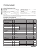
ABSOLUTE MAXIMUM RATINGS
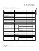
ELECTRICAL CHARACTERISTICS
(VCCA = VCCD = 3.0V, f
CLK
= 15MHz, R
L
= ∞, T
A
= T
MIN
to T
MAX
, unless otherwise noted.)
Stresses beyond those listed under “Absolute Maximum Ratings” may cause permanent damage to the device. These are stress ratings only, and functional
operation of the device at these or any other conditions beyond those indicated in the operational sections of the specifications is not implied. Exposure to
absolute maximum rating conditions for extended periods may affect device reliability.
VCCA to AGND ........................................................-0.3V, +6.0V
VCCD to DGND........................................................-0.3V, +6.0V
VCCA to VCCD...................................................................±6.3V
Digital I/O Pins (D0–D6, CLK, RXEN, TXEN)
to DGND.................................-0.3V to (VCCD + 0.3V) or 6.0V
(whichever is smaller)
Analog I/O Pins (AIO+, AIO-)
to AGND................................(VCCA - 1.5V) to (VCCA + 0.3V)
AGND to DGND........................................................-0.3V, +0.3V
Power Dissipation (T
A
= +70°C)
QSOP (derate 5.90mW/°C above 70°C)......................470mW
Operating Temperature Ranges
MAX1005CEE .....................................................0°C to +70°C
MAX1005EEE...................................................-40°C to +85°C
Storage Temperature Range.............................-65°C to +150°C
Lead Temperature (soldering, <10sec)...........................+300°C
(Notes 9, 10)
AIO+ = AIO-
(Note 4)
(Notes 6, 7)
(Note 3)
(Note 5)
CONDITIONS
-42
dB
-42 -24
THDTotal Harmonic Distortion
mV368 400 432V
IN
Full-Scale Input Range
LSB±2Offset Error
LSB±0.2DNLDifferential Nonlinearity
LSB±0.2INLIntegral Nonlinearity
Bits5NResolution
dB67PSRPower-Supply Rejection
CLK
period
0.5DAC Latency
dBc-50Clock Feedthrough
µs0.7 2.4t
WAKE
Wakeup Time Exiting Shutdown
LSB±0.2 ±1INLIntegral Nonlinearity
Bits7NResolution
-28 dBcTHD+N
Total Harmonic Distortion plus
Noise
39
dBc
28 39
SFDRSpurious-Free Dynamic Range
LSB±0.2 ±1DNLDifferential Nonlinearity
LSB±1Offset Error
mVp-p736 800 864V
OUT
Transmit Full-Scale Output Voltage
UNITSMIN TYP MAXSYMBOLPARAMETER
VCCA = VCCD = 2.7V to 5.5V
VCCA = VCCD = 3.0V
VCCA = VCCD = 3.0V
VCC_ (A or D or both) = 3.0V ±100mVp-p at
100kHz
VCCA = VCCD = 2.7V to 5.5V
VCCA = VCCD = 3.0V
(Note 9)
(Note 9)
4.9
Bits
4.5 4.9
ENOBEffective Number of Bits
44
dB
24 44
SFDRSpurious-Free Dynamic Range
VCCA = VCCD = 2.7V to 5.5V
VCCA = VCCD = 3.0V
VCCA = VCCD = 2.7V to 5.5V
VCCA = VCCD = 3.0V
TRANSMIT DAC DC ACCURACY (Note 1)
TRANSMIT DAC DYNAMIC PERFORMANCE (T
A
= +25°C) (Note 2)
TRANSMIT ADC DC ACCURACY (Note 8)
RECEIVE ADC DYNAMIC PERFORMANCE (T
A
= +25°C) (Note 8)