
Datasheet

CONDITIONS
MAX1005
IF Undersampler
4 _______________________________________________________________________________________
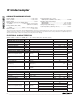
ELECTRICAL CHARACTERISTICS (continued)
(VCCA = VCCD = 3.0V, f
CLK
= 15MHz, R
L
= ∞, T
A
= T
MIN
to T
MAX
, unless otherwise noted.)
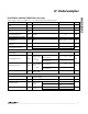
RXEN, TXEN;
VCCD = 2.7V
to 3.6V
D0–D6, CLK; VCCD = 2.7V to 5.5V
C
L
≤ 12.5pF
T
A
= +25°C (Note 6)
T
A
= +25°C (Note 6)
RXEN, TXEN;
VCCD = 3.6V
to 5.5V
D0–D6, CLK; TXEN = 1, RXEN = 0 (Note 6)
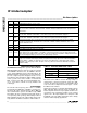
CONDITIONS
±2
±1
µA
-1 7
I
IN
Input Current
ns13 20t
DO
ADC CLK to Output Data Valid
%45 55CLK Duty Cycle
ns5 0.3t
HOLD
DAC Data Hold Time
ns5 0.6t
DS
DAC Data Setup Time
±1
±4
pF8C
IN
Input Capacitance
UNITSMIN TYP MAXSYMBOLPARAMETER
TXEN = 0 and RXEN = 1, or
TXEN = 1 and RXEN = 0
TXEN = RXEN
TXEN = RXEN
TXEN = 0 and RXEN = 1, or
TXEN = 1 and RXEN = 0
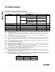
Note 1: TXEN = 1, RXEN = 0. All DAC transfer function parameters are measured differentially from AIO+ to AIO- using the End-
Point Linearity method.
Note 2: f
IN
= 4.3MHz digital sine wave applied to DAC data inputs; f
CLK
= 15MHz. The reference frequency (f
REF
) is defined to be
10.7MHz (f
CLK
- f
IN
). All frequency components present in the DAC output waveform except for f
REF
and f
IN
are consid-
ered spurious.
Note 3: For DAC SFDR measurements, the amplitude of f
REF
(10.7MHz) is compared to the amplitudes of all frequency compo-
nents of the output waveform except for f
IN
(4.3MHz).
Note 4: For DAC measurements, THD+N is defined as the ratio of the square-root of the sum-of-the-squares of the RMS values of
all harmonic and noise components of the output waveform (except for f
IN
and f
REF
) to the RMS amplitude of the f
REF
com-
ponent.
Note 5: Clock feedthrough is defined as the difference in amplitude between the f
REF
component and the f
CLK
component when
measured differentially from AIO+ to AIO-.
Note 6: Guaranteed by design. Not production tested.
Note 7: The DAC input interface is a master/slave register. An additional half clock cycle is required for data at the digital inputs to
propagate through to the DAC switches.
Note 8: RXEN = 1, TXEN = 0. Unless otherwise noted, for all receive ADC measurements, the analog input signal is applied differ-
entially from AIO+ to AIO-, specified using the Best-Fit Straight-Line Linearity method.
Note 9: f
IN
= 10.7MHz, f
CLK
= 15MHz. Amplitude is 1dB below full-scale. The reference frequency (f
REF
) is defined to be 4.3MHz
(f
CLK
- f
IN
). All components except for f
REF
and f
IN
are considered spurious.
Note 10: Receive ADC THD measurements include the first five harmonics.
Note 11: CAUTION: Operation of the analog inputs AIO+ and AIO- (pins 4 and 5) at more than 1.5V below VCCA could cause
latchup and possible destruction of the part. Avoid shunt capacitances to GND on these pins. If shunt capacitances are
required, then bypass these pins only to VCCA.
Note 12: All digital input signals are measured from 50% amplitude reference points. All digital output signal propagation delays are
measured to V
OH(AC)
for rising output signals and to V
OL(AC)
for falling output signals. The values for V
OH(AC)
and V
OL(AC)
as a function of the VCCD supply are shown in the following table:
VCCD (V)
V
OH(AC)
(V) V
OL(AC)
(V)
2.7 to 3.3 VCCD - 1.1 0.5
3.3 to 5.5 2/3 x VCCD 0.5
TIMING CHARACTERISTICS (Data Outputs: R
L
= 1MΩ, C
L
= 15pF, T
A
= T
MIN
to T
MAX
, unless otherwise noted.) (Note 12)