
Datasheet

MAX1005
_______________Detailed Description
The MAX1005 is designed to operate with the Maxim
PWT1900 (TAG-6) wireless transceiver chipset consisting
of the MAX2411 RF transceiver, the MAX2511 IF trans-
ceiver, and the MAX1007 power-control/diversity IC. The
MAX1005 integrates all the functions of an IF undersam-
pler into a single low-power integrated circuit. It is also
well suited for other time-division duplex (TDD) communi-
cations systems. This device includes a 7-bit transmit
DAC, a 5-bit receive ADC, two internal bandgap refer-
ences, clock drivers, and all necessary interface and
control logic.
Transmit DAC
The low-side alias frequency (f
CLK
- f
OUT
= 10.7MHz)
generated by the MAX1005’s 7-bit DAC is used to recre-
ate the IF sub-carrier and transmission data in TDD and
other communications systems. The DAC accepts CMOS
input data in the twos-complement format and outputs a
corresponding analog voltage differentially between
AIO+ and AIO-. The full-scale output voltage range is typ-
ically ±400mV. The DAC code table is shown in Table 1.
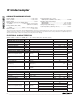
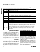
Table 1. Transmit DAC Code Table
Receive ADC
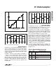
The 5-bit receive ADC is used to directly sample or
undersample a downconverted RF signal. The ADC
converts an analog input signal to a 5-bit digital output
code in the twos-complement format. Figure 1 shows
the ADC transfer function.
Analog input signals are applied differentially between
AIO+ and AIO-, with a full-scale range of ±200mV. An
internal amplifier buffers the input signal and drives the
comparator array, minimizing loading on the external
signal source. The input amplifier has a full-power -1dB
bandwidth of at least 15MHz, making this device ideally
suited for undersampling applications.
IF Undersampler
6 _______________________________________________________________________________________
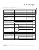
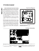
______________________________________________________________Pin Description
Two MSBs for DAC input data. D6 is the MSB.D6, D59, 10
Data Input/Output Pins. If RXEN = 0 and TXEN = 1, then D4–D0 function as the five lower bits of DAC input
data, with D0 as the LSB. If RXEN = 1 and TXEN = 0, then D4–D0 function as the five data outputs for the
ADC, with D4 as the MSB and D0 as the LSB. In low-power shutdown mode (RXEN = TXEN), D0–D4 should
not be externally held high, to prevent excessive input leakage currents.
D4–D011–15
Clock Input. If the receive ADC is active (RXEN = 1, TXEN = 0), the analog input is sampled on the falling
edge of clock and the data outputs (D4-D0) are updated on the rising edge of CLK. If the transmit DAC is
active (TXEN = 1, RXEN = 0), input data is clocked in on the falling edge of CLK and the DAC output is
updated on the rising edge of CLK. The input clock may continue to run when the MAX1005 is shut down
(TXEN = RXEN).
CLK16
Negative Analog Input/Output Pin. If RXEN = 1 and TXEN = 0, then AIO- is the negative analog input to the
receive ADC. If RXEN = 0 and TXEN = 1, then AIO- is the negative transmit DAC output pin.
AIO-5
Transmit DAC Enable Input. A logic-high level on this input combined with a logic-low level on RXEN
enables the transmit DAC and disables the receive ADC. If RXEN = TXEN, the MAX1005 enters its low-
power shutdown mode.
TXEN6
Analog Ground. Connect to analog ground plane.AGND7
Analog Supply Voltage, +2.7V to +5.5VVCCA8
Positive Analog Input/Output Pin. If RXEN = 1 and TXEN = 0, then AIO+ is the positive analog input to the
receive ADC. If RXEN = 0 and TXEN = 1, then AIO+ is the positive transmit DAC output pin.
AIO+4
Receive ADC Enable Input. A logic-high level on this input combined with a logic-low level on TXEN enables
the receive ADC and disables the transmit DAC. If RXEN = TXEN, the MAX1005 enters its low-power shut-
down mode.
RXEN3
PIN
Digital Ground. Connect to digital ground plane.DGND2
Digital Supply Voltage, +2.7V to +5.5VVCCD
1
FUNCTIONNAME
DAC INPUT DATA ANALOG OUTPUT
011 1111 +FS
000 0000 0
100 0000 -FS