
Datasheet

Digital Interface
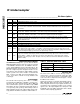
The DAC has a 7-bit parallel digital interface. Figure 2
shows the timing diagram for the transmit DAC. Digital
data is latched into the DAC input register on the falling
edge of CLK. On the next rising edge of CLK the data
is transferred to the DAC register and the DAC output
voltage is updated.
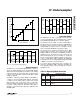
The ADC is enabled by setting TXEN = 0 and RXEN =
1. Figure 3 shows the ADC timing diagram. Input data
is sampled on the falling edge of CLK, while output
data changes state on the rising edge of CLK. This
minimizes digital feedthrough and noise while the ana-
log input is being sampled. The ADC output data is
applied to the 5-bit parallel output pins (D0–D4), with
the MSB at D4.
Operating Modes
The MAX1005 has three operating modes: transmit,
receive, and shutdown. The operating mode is selected
by the RXEN and TXEN inputs, as shown in Table 2.
In transmit mode, the DAC is active and the ADC is
inactive. Power consumption is typically 16.5mW with a
3V supply voltage. In receive mode, the ADC is active
and the DAC is inactive. Power consumption in this
mode is typically 39mW with a 3V supply voltage.
The third mode is shutdown, in which both the DAC
and the ADC are inactive. Select this mode by setting
RXEN = TXEN at any voltage from DGND to VCCD. In
shutdown mode, the CLK input can continue to run
without damaging the device and with no significant
increase in the typical shutdown supply current specifi-
cation of 0.1µA. When exiting shutdown, the MAX1005
is guaranteed to be operational within 2.4µs after TXEN
or RXEN is asserted, as shown in Table 2.
To prevent supply-current drain due to leakage cur-
rents from entering the ADC output bits, the ADC out-
puts (D0–D4) should not be held high in low-power
shutdown mode.
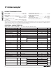
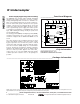
Table 2. Operating Mode Selection
MAX1005
IF Undersampler
_______________________________________________________________________________________ 7
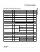
01111
01110
00010
00001
00000
11111
11110
11101
10001
10000
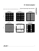
- FS
COM
INPUT VOLTAGE (LSB)
OUTPUT CODE
+FS
Figure 1. Receive ADC Transfer Function
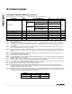
CLK
DAC
OUTPUT
DAC
INPUT
DATA
(D0–D6)
n - 1 n n + 1 n + 2
n - 1 n n + 1
t
DS
t
HOLD
Figure 2. Transmit DAC Timing Diagram
ANALOG
INPUT
D0–D4
CLK
n - 1 n
SAMPLE
n
SAMPLE
n + 1
SAMPLE
n + 2
n + 1
t
DO
Figure 3. Receive ADC Timing Diagram
RXEN TXEN OPERATING MODE
0 0
Low-power shutdown: ADC and DAC
disabled
0 1 Transmit mode: DAC active, ADC disabled
1 0 Receive mode: ADC active, DAC disabled
1 1
Low-power shutdown: ADC and DAC
disabled