
Datasheet

MAX1005
IF Undersampler
Maxim cannot assume responsibility for use of any circuitry other than circuitry entirely embodied in a Maxim product. No circuit patent licenses are
implied. Maxim reserves the right to change the circuitry and specifications without notice at any time.
8
_____________________Maxim Integrated Products, 120 San Gabriel Drive, Sunnyvale, CA 94086 408-737-7600
© 1997 Maxim Integrated Products Printed USA is a registered trademark of Maxim Integrated Products.
Power-Supply Bypassing and Grounding
The MAX1005 has separate analog (VCCA) and digital
(VCCD) power-supply connections, as well as separate
analog and digital ground connections to minimize cou-
pling of noisy digital signals into the circuit’s analog por-
tion. The device will operate with both of these power
supplies connected to any voltage between +2.7V and
+5.5V. This feature allows the digital circuitry to operate
from a regulated logic power supply; this reduces power
consumption and maintains compatibility with external
logic, while allowing the analog circuitry to operate from
an unregulated supply.
The analog ground (AGND) and digital ground (DGND)
should be tied together close to the device. At no time
should the voltage between AGND and DGND exceed
±0.3V.
The entire board needs good DC bypassing for both
analog and digital supplies. Place the power-supply
bypass capacitors close to where the power is routed
onto board. 10µF electrolytic capacitors with low equiva-
lent-series-resistance (ESR) ratings are recommended.
For best effective bits performance, minimize capacitive
loading at the digital outputs. Keep the digital output
traces as short as possible. Bypass each of the VCC_
supply pins to its respective GND with high-quality
ceramic capacitors located as close to the package as
possible.
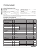
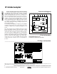
___________________Chip Information
TRANSISTOR COUNT: 2377
SUBSTRATE CONNECTED TO AGND
5-BIT
FLASH ADC
VCCA
5
7
DAC
BANDGAP
REFERENCE
ADC
BANDGAP
REFERENCE
DIGITAL
INTERFACE
TXEN RXEN
ADC
CLOCK
DRIVER
1k 1k
AIO+
AIO-
7-BIT DAC
MAX1005
VCCA AGND VCCD DGND
CLK
DAC
CLOCK
DRIVER
D6–D0
7
________________Functional Diagram
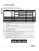
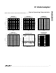
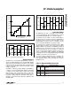
________________________________________________________Package Information
QSOP.EPS