
Datasheet


2 ______________________________________________________________________________________
MAX11205
16-Bit, Single-Channel, Ultra-Low Power,
Delta-Sigma ADC with 2-Wire Serial Interface
Stresses beyond those listed under “Absolute Maximum Ratings” may cause permanent damage to the device. These are stress ratings only, and functional
operation of the device at these or any other conditions beyond those indicated in the operational sections of the specifications is not implied. Exposure to absolute
maximum rating conditions for extended periods may affect device reliability.
Any Pin to GND ....................................................-0.3V to +3.9V
AVDD to GND .......................................................-0.3V to +3.9V
DVDD to GND ......................................................-0.3V to +3.9V
Analog Inputs (AINP, AINN, REFP, REFN)
to GND .............................................. -0.3V to (V
AVDD
+ 0.3V)
Digital Inputs and Digital Outputs
to GND .............................................. -0.3V to (V
DVDD
+ 0.3V)
ESD
HB
(AVDD, AINP, AINN, REFP, REFN, DVDD, CLK, SCLK,
RDY/DOUT, GND) ............................................ Q2kV (Note 1)
Continuous Power Dissipation (T
A
= +70NC)
10-Pin FMAX (derate 5.6mW/NC above +70NC) ..........444mW
Operating Temperature Range .......................... -40NC to +85NC
Junction Temperature .....................................................+150NC
Storage Temperature Range ............................ -55NC to +150NC
Lead Temperature (soldering, 10s) ................................+300NC
Soldering Temperature (reflow) ......................................+260NC
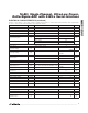
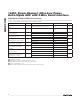
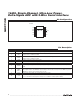
ELECTRICAL CHARACTERISTICS
(V
AVDD
= +3.6V, V
DVDD
= +1.8V, V
REFP
- V
REFN
= V
AVDD
; internal clock, T
A
= T
MIN
to T
MAX
, unless otherwise noted. Typical values
are at T
A
= +25NC under normal conditions, unless otherwise noted.)
ABSOLUTE MAXIMUM RATINGS
Note 1: Human Body Model to specification MIL-STD-883 Method 3015.7.
PARAMETER SYMBOL CONDITIONS MIN TYP MAX UNITS
ADC PERFORMANCE
Noise-Free Resolution NFR (Notes 2, 3) 16 Bits
Thermal Noise (Notes 2, 3) V
N
MAX11205A 2.1
FV
RMS
MAX11205B 0.72
Integral Nonlinearity INL (Note 4) -20 +20 ppmFSR
Zero Error V
OFF
After calibration, V
REFP
- V
REFN
= 2.5V -20 1 +20 ppmFSR
Zero Drift 50 nV/NC
Full-Scale Error
After calibration, V
REFP
- V
REFN
=2.5V
(Note 5)
-45 3 +45 ppmFSR
Full-Scale Error Drift 0.05
ppmFSR/
NC
Power-Supply Rejection
AVDD DC rejection 70 80
dB
DVDD DC rejection (Note 6) 86 100
ANALOG INPUTS/REFERENCE INPUTS
Common-Mode Rejection (Note 6) CMR
DC rejection 90 123
dB50Hz/60Hz rejection, MAX11205A 90
50Hz/60Hz rejection, MAX11205B 144
Normal Mode 50Hz Rejection NMR
50
MAX11205B (Note 7) 65 80.5 dB
Normal Mode 60Hz Rejection NMR
60
MAX11205B (Note 7) 73 87 dB
Common-Mode Voltage Range GND V
AVDD
V
Absolute Input Voltage
Low input voltage
GND -
30mV
V
High input voltage
V
AVDD
+ 30mV
DC Input Leakage Sleep mode (Note 2) ±1 FA
AIN Dynamic Input Current 5 FA