
Datasheet


_______________________________________________________________________________________ 3
MAX11205
16-Bit, Single-Channel, Ultra-Low Power,
Delta-Sigma ADC with 2-Wire Serial Interface
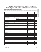
ELECTRICAL CHARACTERISTICS (continued)
(V
AVDD
= +3.6V, V
DVDD
= +1.8V, V
REFP
- V
REFN
= V
AVDD
; internal clock, T
A
= T
MIN
to T
MAX
, unless otherwise noted. Typical values
are at T
A
= +25NC under normal conditions, unless otherwise noted.)
PARAMETER SYMBOL CONDITIONS MIN TYP MAX UNITS
REF Dynamic Input Current 7.5 FA
AIN Input Capacitance 10 pF
REF Input Capacitance 15 pF
AIN Voltage Range V
AINP
- V
AINN
-V
REF
+V
REF
V
REF Voltage Range V
AVDD
V
Input Sampling Rate f
S
MAX11205A 246
kHz
MAX11205B 225
REF Sampling Rate
MAX11205A 246
kHz
MAX11205B 225
LOGIC INPUTS (SCLK, CLK)
Input Current Input leakage current ±1 FA
Input Low Voltage
V
IL
0.3 x
V
DVDD
V
Input High Voltage V
IH
0.7 x
V
DVDD
V
Input Hysteresis V
HYS
200 mV
External Clock
MAX11205A 2.4576
MHz
MAX11205B 2.2528
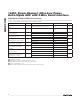
LOGIC OUTPUTS (RDY/DOUT)
Output Low Level V
OL
I
OL
= 1mA; also tested for V
DVDD
= 3.6V 0.4 V
Output High Level V
OH
I
OH
= 1mA; also tested for V
DVDD
= 3.6V
0.9 x
V
DVDD
V
Floating State Leakage Current Output leakage current Q10 FA
Floating State Output
Capacitance
9 pF
POWER REQUIREMENTS
Analog Supply Voltage AVDD 2.7 3.6 V
Digital Supply Voltage DVDD 1.7 3.6 V
Total Operating Current (AVDD + DVDD) 230 300 FA
DVDD Operating Current 45 60 FA
AVDD Operating Current 185 245 FA
AVDD Sleep Current 0.4 2 FA
DVDD Sleep Current 0.35 2 FA
2-WIRE SERIAL-INTERFACE TIMING CHARACTERISTICS
SCLK Frequency f
SCLK
5 MHz
SCLK Pulse Width Low t
1
60/40 duty cycle 5MHz clock 80 ns
SCLK Pulse Width High t
2
40/60 duty cycle 5MHz clock 80 ns
SCLK Rising Edge to Data Valid
Transition Time
t
3
40 ns