
Datasheet


DESIGNATION QTY DESCRIPTION
J1 1 6-pin right-angle male header
JP1 1 3-pin straight male header
R1, R2 2
150I Q5% resistors (0603)
R3, R4, R5 3
33I Q5% resistors (0603)
U1 1
Ultra-low-noise, high-PSRR linear
regulator (5 SC70)
Maxim MAX8510EXK29+
U2 1
16-bit delta-sigma ADC
(10 FMAX
M
)
Maxim MAX11205AEUB+
U3 1
Low-power fixed reference
(5 SOT23)
Maxim MAX6037AAUK25+
— 1 Shorting jumper
— 1 PCB: EPCB11205PM1
SUPPLIER PHONE WEBSITE
Murata Electronics North America, Inc. 770-436-1300 www.murata-northamerica.com
TDK Corp. 847-803-6100 www.component.tdk.com
DESIGNATION QTY DESCRIPTION
C1–C5 5
0.1FF Q10%, 16V X7R ceramic
capacitors (0603)
Murata GRM188R71C104KA01D
C6 1
10FF Q10%, 10V X5R ceramic
capacitor (0603)
TDK C2012X5R1A106K/1.25
C7, C8 2
0.01FF Q10%, 16V X7R ceramic
capacitors (0603)
Murata GRM188R71C103KA01D
C9, C10 2
2.2FF Q10%, 10V X5R ceramic
capacitors (0603)
TDK C1608X5R1A225K/0.80
F1 1
4.7FF EMI filter (3-terminal
capacitor)
Murata NFM21PC475B1A3D
PIN SIGNAL DESCRIPTION
1 N.C. Not connected
2 N.C. Not connected
3 MISO
Data-ready output/serial-data output.
This output serves a dual function.
In addition to the serial-data output
function, the MISO pin also indicates
that the data is ready when it is pulled
logic-low by the IC. Output data
changes on the falling edge of SCLK.
4 SCK
2-wire serial clock. The host must apply
an external clock signal to shift data
out from the IC.
5 GND Ground
6 VCC Power supply
_________________________________________________________________ Maxim Integrated Products 2
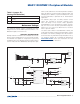
MAX11205PMB1 Peripheral Module
Detailed Description
2-Wire Interface
The MAX11205PMB1 peripheral module interfaces with
a host using a 2-wire serial interface. When an ADC
conversion is complete, the IC pulls the data line low.
The host must then supply a clock signal to shift out the
conversion data. More information on the 2-wire interface
can be found the MAX11205 IC data sheet.
Connector J1 provides connection of the module to the
Pmod host. See Table 1.
Jumper JP1 allows the user to select between two volt-
ages for IC analog supply voltage (AVDD). This allows
the option of applying additional power-supply filtering
based on the noise content of the incoming voltage
source (connector J1) and the performance require-
ments for the application. See Table 2.
Component Suppliers
Note: Indicate that you are using the MAX11205PMB1 when contacting these component suppliers.
Component List
Table 1. Connector J1 (2-Wire Communication)
µMAX is a registered trademark of Maxim Integrated Products,
Inc.