
Datasheet


MAX13046E/MAX13047E
typical application involves interfacing a low-voltage
microprocessor to an external memory, such as the
DS2502. The maximum data rate depends on the
1-Wire device. For the DS2502, the maximum data rate
is 16.3kbps. A 5kΩ pullup resistor is recommended
when interfacing with the DS2502.
Push-Pull vs. Open-Drain Driving
The MAX13046E/MAX13047E can be driven in a push-
pull or open-drain configurations. For open-drain con-
figuration, internal 10kΩ resistors pull up I/O V
L
and I/O
V
CC
to their respective power supplies. See the
Timing
Characteristics
table for maximum data rates when
using open-drain drivers.
PCB Layout
The MAX13046E/MAX13047E require good PCB layout
for proper operation and optimal rise/fall time perfor-
mance. Ensure proper high-frequency PCB layout even
when operating at low data rates.
Driving High-Capacitive Load
Capacitive loading on the I/O lines impacts the rise time
(and fall time) of the MAX13046E/MAX13047E when dri-
ving the signal lines. The actual rise time is a function of
the load capacitance, parasitic capacitance, the supply
voltage, and the drive impedance of the MAX13046E/
MAX13047E.
Operating the MAX13046E/MAX13047E at a low data rate
does NOT increase capacitive load driving capability.
Single- and Dual-Bidirectional
Low-Level Translator
12 ______________________________________________________________________________________
I
P
100%
90%
36.8%
t
RL
TIME
t
DL
CURRENT WAVEFORM
PEAK-TO-PEAK RINGING
(NOT DRAWN TO SCALE)
I
r
10%
0
0
AMPERES
Figure 2b. Human Body Current Waveform
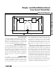
CHARGE-CURRENT-
LIMIT RESISTOR
DISCHARGE
RESISTANCE
STORAGE
CAPACITOR
C
s
100pF
R
C
1MΩ
R
D
1500Ω
HIGH-
VOLTAGE
DC
SOURCE
DEVICE
UNDER
TEST
Figure 2a. Human Body ESD Test Model
100%
90%
60ns
10%
tr = 0.7ns TO 1ns
I
PEAK
I
30ns
t
Figure 3b. IEC 61000-4-2 ESD Generator Current Waveform
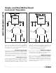
CHARGE-CURRENT-
LIMIT RESISTOR
DISCHARGE
RESISTANCE
STORAGE
CAPACITOR
C
s
150pF
R
C
50MΩ TO 100MΩ
R
D
330Ω
HIGH-
VOLTAGE
DC
SOURCE
DEVICE
UNDER
TEST
Figure 3a. IEC 61000-4-2 ESD Test Model