
Datasheet


MAX13046E/MAX13047E
Detailed Description
The MAX13046E/MAX13047E ±15kV ESD-protected
bidirectional level translators provide level shifting for
data transfer in a multivoltage system. The MAX13046E
is a single-channel translator and the MAX13047E is a
dual-channel translator. Externally applied voltages,
V
CC
and V
L
, set the logic level on either side of the
device. The MAX13046E/MAX13047E utilize a transmis-
sion-gate-based design to allow data translation in
either direction (V
L
↔ V
CC
) on any single data line. The
MAX13046E/MAX13047E accept V
L
from +1.1V to the
minimum of either +3.6V or (V
CC
+ 0.3V) and V
CC
from
+1.65V to +5.5V, making these devices ideal for data
transfer between low-voltage ASICs/PLDs and higher
voltage systems.
The MAX13046E/MAX13047E feature a shutdown mode
that reduces supply current to less than 1µA thermal
short-circuit protection, and ±15kV ESD protection on the
V
CC
side for enhanced protection in applications that
route signals externally. The MAX13046E/MAX13047E
operate at a guaranteed data rate of 8Mbps when push-
pull driving is used. See the
Functional Diagram
.
Single- and Dual-Bidirectional
Low-Level Translator
8 _______________________________________________________________________________________
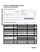
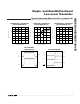
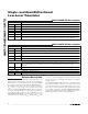
MAX13046E Pin Description
MAX13046E FUNCTION
µDFN
NAME
1V
L
V
L
Inp ut S up p l y V ol tag e. Byp ass V
L
w i th a 0.1µF cer am i c cap aci tor l ocated as cl ose as p ossi b l e to the i np ut.
2 GND Ground
3 I/O V
L
Input/Output. Referenced to V
L
.
4
I/O V
CC
Input/Output. Referenced to V
CC
.
5 SHDN S hutd ow n Inp ut. D r i ve S HD N hi g h to enab l e the d evi ce. D r i ve S HD N l ow to p ut the d evi ce i n shutd ow n m od e.
6V
CC
V
CC
Inp ut S up p l y V ol tag e. Byp ass V
CC
w i th a 1µF cer am i c cap aci tor l ocated as cl ose as p ossi b l e to the i np ut
for ful l E S D p r otecti on. If ful l E S D p r otecti on i s not r eq ui r ed , b yp ass V
CC
w i th a 0.1µF cer am i c cap aci tor .
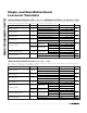
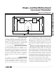
MAX13047E Pin Description
MAX13047E FUNCTION
UTQFN NAME
1
I/O V
L2
Input/Output 2. Referenced to V
L
.
2V
L
V
L
Input Supply Voltage. Bypass V
L
with a 0.1µF ceramic capacitor located as close as possible to the
input.
3, 7 N.C. Not Connected. Internally not connected.
4 SHDN Enable Input. Drive SHDN high to enable the device. Drive SHDN low to put the device in shutdown mode.
5
I/O V
CC2
Input/Output 2. Referenced to V
CC
.
6V
CC
V
CC
Input Supply Voltage. Bypass V
CC
with a 1µF ceramic capacitor located as close as possible to the
input for full ESD protection. If full ESD protection is not required, bypass V
CC
with a 0.1µF ceramic
capacitor.
8
I/O V
CC1
Input/Output 1. Referenced to V
CC
.
9 GND Ground
10
I/O V
L1
Input/Output 1. Referenced to V
L
.
— EP Exposed Pad. Connect EP to GND.