
Datasheet


MAX13202E/MAX13204E/MAX13206E/MAX13208E
2-/4-/6-/8-Channel, ±30kV ESD Protectors in µDFN
2 _______________________________________________________________________________________
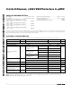
ABSOLUTE MAXIMUM RATINGS
ELECTRICAL CHARACTERISTICS
(V
CC
= +5V ±5%, T
A
= T
MIN
to T
MAX
, unless otherwise noted. Typical values are at V
CC
= +5V and T
A
= +25°C.) (Note 1)
Stresses beyond those listed under “Absolute Maximum Ratings” may cause permanent damage to the device. These are stress ratings only, and functional
operation of the device at these or any other conditions beyond those indicated in the operational sections of the specifications is not implied. Exposure to
absolute maximum rating conditions for extended periods may affect device reliability.
Note 1: Limits over temperature are guaranteed by design, not production tested.
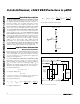
Note 2: Idealized clamp voltages (L1 = L2 = L3 = 0) (Figure 1); see the Applications Information section for more information.
Note 3: Guaranteed by design. Not production tested.
V
CC
to GND............................................................-0.3V to +18V
I/O_ to GND................................................-0.3V to (V
CC
+ 0.3V)
Continuous Power Dissipation (T
A
= +70°C)
6-Pin, 1mm x 1.5mm µDFN (derate 2.1mW/°C
above +70°C)................................................................168mW
6-Pin, 2mm x 2mm µDFN (derate 4.5mW/°C
above +70°C)................................................................358mW
8-Pin, 2mm x 2mm µDFN (derate 4.8mW/°C
above +70°C)................................................................381mW
10-Pin, 2mm x 2mm µDFN (derate 5.0mW/°C
above +70°C)................................................................403mW
Operating Temperature Range .........................-40°C to +125°C
Storage Temperature Range .............................-65°C to +150°C
Junction Temperature .....................................................+150°C
Lead Temperature (soldering, 10s) .................................+300°C
PARAMETER
SYMBOL
CONDITIONS
MIN
TYP
MAX
UNITS
Supply Voltage V
CC
0.9
16.0
V
Supply Current I
CC
1 100 nA
Diode Forward Voltage V
F
I
F
= 10mA
0.65 0.95
V
Positive transients
V
CC
+ 25
T
A
= +25°C, ±15kV,
Human Body Model,
I
F
= 10A
Negative transients
-25
Positive transients
V
CC
+ 80
T
A
= +25°C, ±14kV,
Contact Discharge
(IEC 61000-4-2), I
F
= 42A
Negative transients
-80
Positive transients
V
CC
+ 120
Channel Clamp Voltage
(Note 2)
V
C
T
A
= +25°C, ±30kV,
Air-Gap Discharge
(IEC 61000-4-2), I
F
= 90A
Negative transients -120
V
T
A
= -40°C to +50°C -1 +1 nA
Channel Leakage Current
(Note 3)
T
A
= -40°C to +125°C -1 +1 µA
Channel Input Capacitance
V
CC
= 5V, bias of V
CC
/2, f = 1MHz (Note 3) 6 7 pF
ESD PROTECTION
Human Body Model
±15
kV
MAX13204E/MAX13206E/MAX13208E
±14
IEC 61000-4-2
Contact Discharge
MAX13202E
±12
kV
IEC 61000-4-2
Air-Gap Discharge
±30
kV