
Datasheet


SUPPLIER PHONE WEBSITE
Fairchild Semiconductor 888-522-5372 www.fairchildsemi.com
HALO Electronics, Inc. 650-903-3800 www.haloelectronics.com
Murata Electronics North America, Inc. 770-436-1300 www.murata-northamerica.com
_________________________________________________________________ Maxim Integrated Products 2
MAX13256 Evaluation Kit
Evaluates: MAX13256
Quick Start
Required Equipment
• MAX13256EVkit
• +24V,1ADCpowersupply
• Electronicloadcapableof200mA
• Ammeter
• Voltmeter
Procedure
The EV kit is fully assembled and tested. Follow the steps
below to verify board operation. Caution: Do not turn on
the power until all connections are completed.
1) Verify that jumpers JU1, JU2, and JU4 are in their
default positions, as shown in Tables 1, 2, and 3.
2) Set the DC power supply to 24V.
3) Set the electronic load to 200mA and disable
the output.
4) Connect the voltmeter between the +VOUT and
SGND PCB pads on the EV kit.
5) Connect the ammeter between the +VOUT PCB
pad on the EV kit and the positive terminal on the
electronic load. The negative terminal on the
electronic load is connected to the SGND PCB pad
on the EV kit.
6) Connect the power supply between the VDD and
GND PCB pads on the EV kit.
7) Turn on the power supply.
8) Enable the electronic load.
9) Verify that the ammeter reads approximately 200mA.
10) Verify that the voltmeter reads approximately 22.8V.
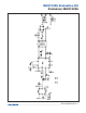
Detailed Description
The MAX13256 EV kit is a 10W, isolated H-bridge DC-DC
converter that provides an unregulated output that is
two diode-voltage drops less than its input supply,
with respect to the isolated ground. In the default
configuration, the maximum load is limited by the device
and the on-board transformer.
The device is an integrated primary-side controller
and H-bridge driver for isolated power-supply circuits.
The device contains an on-board oscillator, protec-
tion circuitry, and internal MOSFETs to provide up to
300mA of current to the transformer’s primary winding.
The device can be operated using the internal 425kHz
oscillator, or driven by an external clock to synchronize
multiple devices and control EMI behavior. Regardless
of the clock source being used, an internal flip-flop
stage guarantees a fixed 50% duty cycle, preventing DC
current flow in the transformer as long as the clock’s
period is constant.
The device operates from a single-supply voltage and
includes UVLO and an active-low enable input for
controlled startup. If the input voltage at VDD falls below
6.3V, or the EN input is pulled above 2V, the device shuts
down and ST1 and ST2 are high impedance.
The device features an adjustable output current limit
at the transformer driver outputs (ST1 and ST2). When
the current reaches the limit for longer than the 1.2ms
blanking time, the drive outputs are disabled and
the FAULT output asserts. The drivers are reenabled
after the 38.2ms autoretry time. If a continuous fault
condition is present, the duty cycle of the fault current is
approximately 3%.
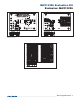
The EV kit PCB is designed for 1500V
RMS
isolation,
with 300 mil spacing between the GND and SGND
planes. The bottom PCB GND plane under device U1
is utilized as a thermal heatsink for power dissipation
of the device’s thermally enhanced TDFN package with
exposed pad. Test points GND and SGND are provided
on the PCB for probing the respective ground planes, or
to connect the GND and SGND planes for nonisolated
evaluation of the circuit.
Clock Source
The device has two modes of operation: internal
oscillator or external clock. To use the internal 425kHz
oscillator, place a shunt in the 1-2 position on jumper
JU2. When using an external clock, remove the shunt
from JU2 and apply a clock signal on the CLK PCB
pad on the EV kit. An internal flip-flop divides the
external clock by two, generating a switching signal with a
guaranteed 50% duty cycle. As a result, the device
outputs switch at 1/2 the external clock frequency.
Component Suppliers
Note: Indicate that you are using the MAX13256 when contacting these component suppliers.