
Datasheet


2 Maxim Integrated
Adjustable Overvoltage and Overcurrent
Protectors with High Accuracy
MAX14571/MAX14572/MAX14573
Stresses beyond those listed under “Absolute Maximum Ratings” may cause permanent damage to the device. These are stress ratings only, and functional
operation of the device at these or any other conditions beyond those indicated in the operational sections of the specifications is not implied. Exposure to absolute
maximum rating conditions for extended periods may affect device reliability.
(All voltages referenced to GND.)
IN, HVEN ................................................................-40V to +40V
IN to OUT ...............................................................-40V to +40V
OUT ......................................................................-0.3V to +40V
OVLO, UVLO, FLAG, EN, RIEN ............................-0.3V to +6.0V
Current into IN (DC Operating) (Note 1) .............. ………….4.2A
SETI .......................... ………….-0.3V to Min (V
IN
, 1.22V) + 0.3V
Continuous Power Dissipation (T
A
= +70NC)
TSSOP (derate 25.6mW/NC above +70NC)........ ….2051.3mW
Operating Temperature Range .......................... -40NC to +85NC
Junction Temperature ........................................………..+150NC
Storage Temperature Range ............................ -65NC to +150NC
Lead Temperature (soldering, 10s) ................. …………+300NC
Soldering Temperature (reflow) ....................... …………+260NC
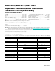
ELECTRICAL CHARACTERISTICS
(V
IN
= 4.5V to 36V, T
A
= -40NC to +85NC, unless otherwise noted. Typical values are at V
IN
= 24V, R
ISET
= 12kI, T
A
= +25°C.) (Note 3)
ABSOLUTE MAXIMUM RATINGS
PACKAGE THERMAL CHARACTERISTICS (Note 2)
Note 1: DC current is also limited by the thermal design of the system.
TSSOP
Junction-to-Ambient Thermal Resistance (B
JA
) ........... +39NC/W
Junction-to-Case Thermal Resistance (B
JC
) .................. +3NC/W
Note 2: Package thermal resistances were obtained using the method described in JEDEC specification JESD51-7, using a four-layer
board. For detailed information on package thermal considerations, refer to www.maximintegrated.com/thermal-tutorial.
PARAMETER SYMBOL CONDITIONS MIN TYP MAX UNITS
IN Voltage Range V
IN
4.5 36 V
Shutdown Input Current I
SHDN
V
EN
= 0V, V
HVEN
= 5V
15
FA
Shutdown Output Current I
OFF
V
OUT
= 0V 2
FA
Reverse Input Current I
IN_RVS
V
IN
= -40V, V
OUT
= V
GND
= 0V -35
FA
Supply Current I
IN
V
IN
= 15V, R
ISET
= 12kI
490 700
FA
Internal Overvoltage Trip Level V
OVLO
V
IN
rising 32 33 34
V
V
IN
falling 32
Internal Undervoltage Trip Level V
UVLO
V
IN
falling 17.5 18.5 19.5
V
V
IN
rising 18.2 19.2 20.2
Overvoltage-Lockout Hysteresis % of typical OVLO 3 %
External OVLO Adjustment Range (Note 4) 6 36 V
External OVLO Select Voltage V
OVLOSEL
0.3 0.50 V
External OVLO Leakage Current I
OVLO_LEAK
V
OVLO
< 1.2V (Note 5) -100 +100 nA
External UVLO Adjustment Range 4.5 24 V
External UVLO Select Voltage V
OVLOSEL
0.3 0.50 V
External UVLO Leakage Current I
UVLO_LEAK
(Note 5) -100 +100 nA
BG Reference Voltage V
BG
1.186 1.210 1.234 V