
Datasheet


Calculate the reset timeout period as follows:
where V
TH-RESET
is 0.5V, I
CH-RESET
is 0.5µA, t
RP
is in
seconds, and C
CRESET
is in Farads. To ensure timing
accuracy and proper operation, minimize leakage at
C
CRESET
.
Adjustable Delay (CDLY_)
When V
IN
rises above V
TH
with EN_ high, the internal
250nA current source begins charging an external
capacitor connected from CDLY_ to GND. When the
voltage at CDLY_ reaches 1V, OUT_ goes high. When
OUT_ goes high, CDLY_ is immediately held low.
Adjust the delay (t
DELAY
) from when V
IN
rises above
V
TH
(with EN_ high) to OUT_ going high according to
the equation:
where V
TH-CDLY
is 1V, I
CH-CDLY
is 0.25µA, C
CDLY
is in
Farads, t
DELAY
is in seconds, and t
DELAY+
is the inter-
nal propagation delay of the device. To ensure timing
accuracy and proper operation, minimize leakage
at CDLY.
Manual-Reset Input (
MR
)
Many µP-based products require manual-reset capabil-
ity, allowing the operator, a test technician, or external
logic circuitry to initiate a reset. A logic-low on MR
asserts RESET low. RESET remains asserted while MR
is low and during the reset timeout period (140ms fixed
or capacitor adjustable) after MR returns high. The MR
input has a 500nA internal pullup, so it can be left
unconnected, if not used. MR can be driven with TTL or
CMOS logic levels, or with open-drain/collector outputs.
Connect a normally open momentary switch from MR to
GND to create a manual-reset function. External
debounce circuitry is not required. If MR is driven from
long cables or if the device is used in a noisy environ-
ment, connect a 0.1µF capacitor from MR to GND to
provide additional noise immunity.
Pullup Resistor Values
The exact value of the pullup resistors for the open-
drain outputs is not critical, but some consideration
should be made to ensure the proper logic levels
when the device is sinking current. For example, if
V
CC
= 2.25V and the pullup voltage is 28V, keep the
sink current less than 0.5mA as shown in the
Electrical
Characteristics
table. As a result, the pullup resistor
should be greater than 56kΩ. For a 12V pullup, the
resistor should be larger than 24kΩ. Note that the ability
to sink current is dependent on the V
CC
supply voltage.
Power-Supply Bypassing
The device operates with a V
CC
supply voltage from
2.2V to 28V. When V
CC
falls below the UVLO threshold,
all the outputs go low and stay low until V
CC
falls below
1.2V. For noisy systems or fast rising transients on V
CC
,
connect a 0.1µF ceramic capacitor from V
CC
to GND
as close to the device as possible to provide better
noise and transient immunity.
Ensuring Valid Output with V
CC
Down to
0V (MAX16026/MAX16028/MAX16030 Only)
When V
CC
falls below 1.2V, the ability for the output to
sink current decreases. In order to ensure a valid out-
put as V
CC
falls to 0V, connect a 100kΩ resistor from
OUT/RESET to GND.
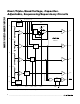
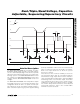
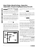
Typical Application Circuits
Figures 4 and 5 show typical applications for the
MAX16025–MAX16030. In high-power applications,
using an n-channel device reduces the loss across the
MOSFETs as it offers a lower drain-to-source on-resis-
tance. However, an n-channel MOSFET requires a suffi-
cient V
GS
voltage to fully enhance it for a low R
DS_ON
.
The application in Figure 4 shows the MAX16027 con-
figured in a multiple-output sequencing application.
Figure 5 shows the MAX16029 in a power-supply
sequencing application using n-channel MOSFETs.
t
V
I
C
DELAY
TH CDLY
CH CDLY
CDLY
=×+×
−
−
−
35 10
6
t
V
I
C
RP
TH RESET
CH RESET
CRESET
=×+×
−
−
−
35 10
6
MAX16025–MAX16030
Dual-/Triple-/Quad-Voltage, Capacitor-
Adjustable, Sequencing/Supervisory Circuits
______________________________________________________________________________________ 11