
Datasheet

MAX16025–MAX16030
Dual-/Triple-/Quad-Voltage, Capacitor-
Adjustable, Sequencing/Supervisory Circuits
_______________________________________________________________________________________ 7
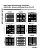
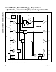
Pin Description (continued)
PIN
MAX16025/
MAX16026
MAX16027/
MAX16028
MAX16029/
MAX16030
NAME FUNCTION
11 14 17 OUT1
Output 1. When the voltage at IN1 is below its threshold or EN1 goes low,
OUT1 goes low.
12 15 18 RESET
Active-Low Reset Output. RESET asserts low when any of the monitored
voltages (IN_) falls below its respective threshold, any EN_ goes low, or MR is
asserted. RESET remains asserted for the reset timeout period after all of the
monitored voltages exceed their respective threshold, all EN_ are high, all
OUT_ are high, and MR is deasserted.
13 16 19 MR
Active-Low Manual Reset Input. Pull MR low to assert RESET low. RESET
remains low for the reset timeout period after MR is deasserted (as long as all
OUT_ are high).
14 17 20 CRESET
Capacitor-Adjustable Reset Delay Input. Connect an external capacitor from
CRESET to GND to set the reset timeout period or connect to V
CC
for the
default 140ms minimum reset timeout period. Leave CRESET open for internal
propagation delay.
— — 21 CDLY4
Capacitor-Adjustable Delay Input 4. Connect an external capacitor from
CDLY4 to GND to set the IN4 to OUT4 (and EN4 to OUT4) delay period.
Leave CDLY4 open for internal propagation delay.
— 18 22 CDLY3
Capacitor-Adjustable Delay Input 3. Connect an external capacitor from
CDLY3 to GND to set the IN3 to OUT3 (and EN3 to OUT3) delay period.
Leave CDLY3 open for internal propagation delay.
15 19 23 CDLY2
Capacitor-Adjustable Delay Input 2. Connect an external capacitor from
CDLY2 to GND to set the IN2 to OUT2 (and EN2 to OUT2) delay period.
Leave CDLY2 open for internal propagation delay.
16 20 24 CDLY1
Capacitor-Adjustable Delay Input 1. Connect an external capacitor from
CDLY1 to GND to set the IN1 to OUT1 (and EN1 to OUT1) delay period.
Leave CDLY1 open for internal propagation delay.
———EP
Exposed Pad. EP is internally connected to GND. Connect EP to the
ground plane.
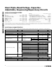
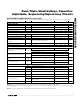
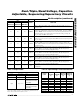
Table 1. Output State*
EN_ IN_ OUT_
Low V
IN_
< V
TH
Low
High V
IN_
< V
TH
Low
Low V
IN_
> V
TH
Low
OUT_ = high
(MAX16026/MAX16028/
MAX16030)
High V
IN_
> V
TH
OUT_ = high impedance
(MAX16025/MAX16027/
MAX16029)
Table 2. Input-Voltage Threshold Selector
TH1/TH0
LOGIC
IN1 (ALL
VERSIONS)
(V)
IN2 (ALL
VERSIONS)
(V)
IN3
(MAX16027/
MAX16028)
(V)
IN4
(MAX16029/
MAX16030)
(V)
Low/Low 3.3 2.5 1.8 1.5
Low/High 3.3 1.8 Adj Adj
Low/Open 3.3 1.5 Adj Adj
High/Low 3.3 1.2 1.8 2.5
High/High 2.5 1.8 Adj Adj
High/Open 3.3 Adj 2.5 Adj
Open/Low 3.3 Adj Adj Adj
Open/High 2.5 Adj Adj Adj
Open/Open Adj Adj Adj Adj
*
When V
CC
falls below the UVLO, all outputs go low regardless
of the state of EN_ and V
IN_
. The outputs are guaranteed to be
in the correct state for V
CC
down to 1.2V.